REV. D
AD641
–12–
Using Higher Supply Voltages
The AD641 is calibrated using ±5 V supplies. Scaling is very
insensitive to the supply voltages and higher supply voltages will
not directly cause significant errors. However, the AD641 power
dissipation must be kept below 500 mW in the interest of reli-
ability and long term stability. When using well regulated supply
voltages above ±6 V, the decoupling resistors shown in the
application schematics can be increased to maintain ±5 V at the
IC. The resistor values are calculated using the specified maxi-
mum of 15 mA current into the +V
S
terminal (Pin 12) and a
maximum of 60 mA into the –V
S
terminal (Pin 7). For example,
when using ±9 V supplies, a resistor of (9 V – 5 V)/15 mA, about
261 , should be included in the +V
S
lead to each AD641 and
(9 V – 5 V)/60 mA, about 64.9 in each –V
S
lead. Of course,
asymmetric supplies may be dealt with in a similar way.
Using the Attenuator
In applications where the signal amplitude is sufficient, the on-
chip attenuator should be used because it provides a tempera-
ture independent dynamic range (compare Figures 18 and 19).
Figure 26 shows this attenuator in more detail. R1 is a thin-film
4
17
3
18
2
19
1
20
5
ATN
COM
16
SIG
–IN
SIG
+IN
ATN
COM
ATN
LO
ATN
IN
R3
R4
R1
R2
ATN
OUT
FIRST
AMPLIFIER
INPUT
Figure 26. Details of the Input Attenuator
resistor of nominally 270 and low temperature coefficient
(TC). It is trimmed to calibrate the intercept to 10 mV dc (or
–24 dBm for sinusoidal inputs), that is, to an attenuation of
nominally 20 dBs at +27°C. R2 has a nominal value of 30 and
has a high positive TC, such that the overall attenuation factor
is 0.33%/°C at +27°C. This results in a transmission factor that is
proportional to absolute temperature, or PTAT. (See Intercept
Stabilization for further explanation.) To improve the accuracy
of the attenuator, the ATN COM nodes are bonded to both Pin
3 and Pin 4. These should be connected directly to the “SlGNAL
LOW” of the source (for example, to the grounded side of the
signal connector, as shown in Figure 32) not to an arbitrary
point on the ground plane.
R4 is identical to R2, and in shunt with R3 (270 thin film)
forms a 27 resistor with the same TC as the output resistance
of the attenuator. By connecting Pin 1 to ATN LOW (Pin 2)
this resistance minimizes the offset caused by bias currents. The
offset nulling scheme shown in Figure 25 may still be used, with
the external resistor R
B
omitted and R
OS
= 500 k. Offset stabil-
ity is improved because the compensating voltage introduced at
Pin 20 is now PTAT. Drifts of under 1 µV/°C (referred to Pins
1 and 20) can be maintained using the attenuator.
It may occasionally be desirable to attenuate the signal even
further. For example, the source may have a full-scale value of
±10 V, and since the basic range of the AD641 extends only to
±200 mV dc, an attenuation factor of ×50 might be chosen.
This may be achieved either by using an independent external
attenuator or more simply by adding a resistor in series with
ATN IN (Pin 5). In the latter case the resistor must be trimmed
to calibrate the intercept, since the input resistance at Pin 5 is
not guaranteed. A fixed resistor of 1 k in series with a 500
variable resistor calibrate to an intercept of 50 mV (or –26 dBV)
for dc or square wave inputs and provide a ±10 V input range.
The intercept stability will be degraded to about 0.003 dB/°C.
NC
DENOTES A CONNECTION TO THE
GROUND PLANE; OBSERVE COMMON
CONNECTIONS WHERE SHOWN.
ALL UNMARKED CAPACITORS ARE
0.1mF CERAMIC. FOR VALUES OF
NUMBERED COMPONENTS SEE TEXT
10V
NC
NC
R1
R2
SIGNAL
INPUT
C1
C2
4.7V
4.7V
–5V
+5V
1mA/DECADE
OUTPUT
–50mV/DECADE
C3
R
L
= 50V
9
87
6
10
53214
12
1314
15
11
16181920 17
LOG
OUT
LOG
COM
SIG
+OUT
RG2
–V
S
SIG
–OUT
RG0RG1CKT
COM
ATN
OUT
SIG
+IN
+V
S
ITCBL1
ATN
IN
ATN
COM
ATN
COM
ATN
LO
SIG
–IN
BL2
1kV
1kV
U1 AD641
9
87
6
10
53214
12
1314
15
11
16181920 17
LOG
OUT
LOG
COM
SIG
+OUT
RG2
–V
S
SIG
–OUT
RG0RG1CKT
COM
ATN
OUT
SIG
+IN
+V
S
ITCBL1
ATN
IN
ATN
COM
ATN
COM
ATN
LO
SIG
–IN
BL2
1kV
1kV
U2 AD641
10V 10V 10V
Figure 27. Basic Connections for Cascaded AD641s
REV. D
AD641
–13–
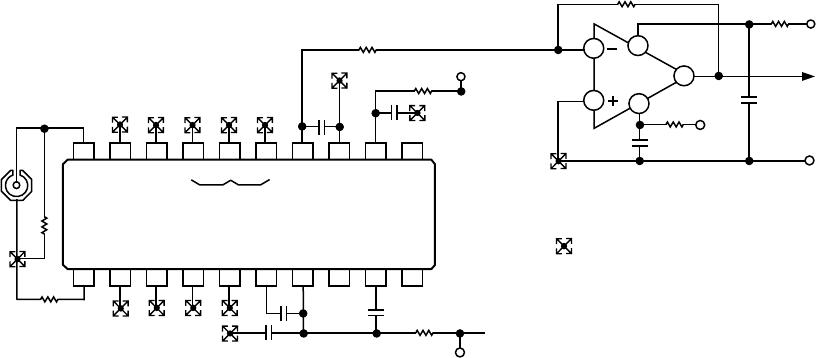
OPERATION OF CASCADED AD641S
Frequently, the dynamic range of the input will be 50 dB or
more. Two AD641s can be cascaded, as shown in Figure 27.
The balanced signal output from U1 becomes the input to U2.
Resistors are included in series with each LOG OUT pin and
capacitors C1 and C2 are placed directly between Pins 13 and 14
to provide a local path for the RF current at these output pairs.
C1 through C3 are chosen to provide the required low pass
corner in conjunction with the load R
L
. Board layout and
grounding disciplines are critically important at the high gain
(X100,000) and bandwidth (~ 150 MHz) of this system.
The intercept voltage is calculated as follows. First, note that if
its LOG OUT is disconnected, U1 simply inserts 50 dB of gain
ahead of U2. This would lower the intercept by 50 dB, to
–110 dBV for square wave calibration. With the LOG OUT of
U1 added in, there is a finite zero signal current which slightly
shifts the intercept. With the intercept temperature compensa-
tion on U1 disabled this zero signal output is –270 µA equiva-
lent to a 5.4 dB upward shift in the intercept, since the slope is
50 µA/dB. Thus, the intercept is at –104.6 dBV (–88 dBm for
50 sine calibration). ITC may be disabled by grounding Pin 8
of either U1 or U2.
Cascaded AD641s can be used in dc applications, but input
offset voltage will limit the dynamic range. The dc intercept is
6 µV. The offset should not be confused with the intercept, which is
found by extrapolating the transfer function from its central “log
linear” region. This can be understood by referring to Equation
(1) and noting that an input offset is simply additive to the value
of V
IN
in the numerator of the logarithmic argument; it does not
affect the denominator (or intercept) V
X
. In dc coupled applica-
tions of wide dynamic range, special precautions must be taken
to null the input offset and minimize drift due to input bias
offset. It is recommended that the input attenuator be used,
providing a practical input range of –74 dBV (±200 µV dc) to
+6 dBV (±2 V dc) when nulled using the adjustment circuit
shown in Figure 25.
1920
21
U2
12
11
910
U1
1920
21
U2
12
11
910
U1
(a)
(
b
)
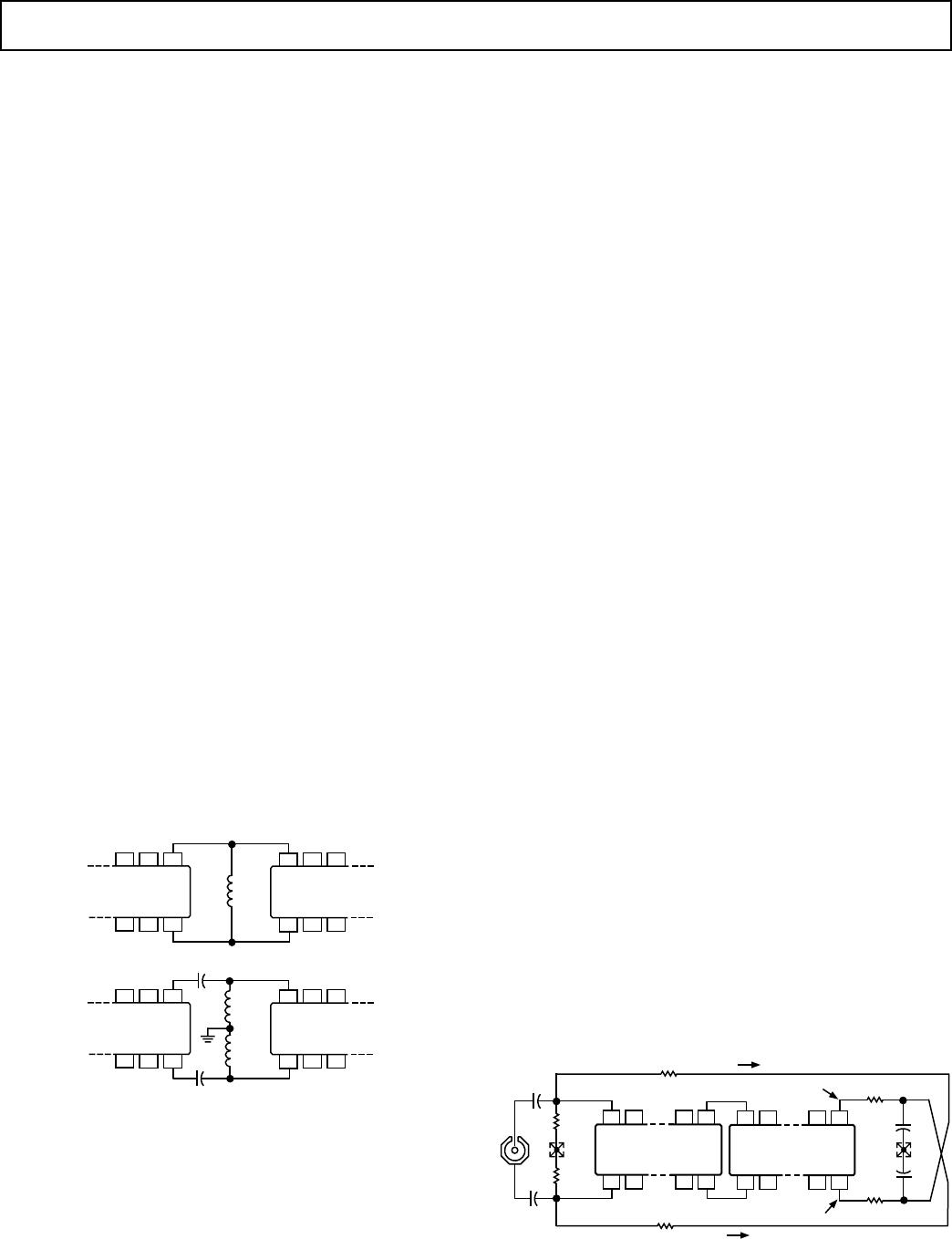
Figure 28. Two Methods for AC Coupling AD641s
Eliminating the Effect of First Stage Offset
Usually, the input signal will be sinusoidal and U1 and U2 can
be ac coupled. Figure 28a shows a low resistance choke at the
input of U2 which shorts the dc output of U1 while preserving
the hf response. Coupling capacitors may be inserted (Figure
28b) in which case two chokes are used to provide bias paths for
U2. These chokes must exhibit high impedance over the operat-
ing frequency range.
Alternatively, the input offset can be nulled by a negative feed-
back network from the SIG OUT nodes of U2 to the SIG IN
nodes of U1, as shown in Figure 29. The low pass response of
the feedback path transforms to a closed-loop high pass response.
The high gain (×100,000) of the signal path results in a com-
mensurate reduction in the effective time constant of this net-
work. For example, to achieve a high pass corner of 100 kHz,
the low pass corner must be at 1 Hz.
In fact, it is somewhat more complicated than this. When the ac
input sufficiently exceeds that of the offset, the feedback be-
comes ineffective and the response becomes essentially dc
coupled. Even for quite modest inputs the last stage will be
limiting and the output (Pins 10 and 11) of U2 will be a square
wave of about ±180 mV amplitude, dwelling approximately
equal times at its two limit values, and thus having a net average
value near zero. Only when the input is very small does the high
pass behavior of this nulling loop become apparent. Consequently,
the low pass time constant can usually be reduced considerably
without serious performance degradation.
The resistor values are chosen such that the dc feedback is
adequate to null the worst case input offset, say, 500 µV. There
must be some resistance at Pins 1 and 20 across which the offset
compensation voltage is developed. The values shown in the
figure assume that we wish to terminate a 50 source at Pin 20.
The 50 resistor at Pin 1 is essential, both to minimize offsets
due to bias current mismatch and because the outputs at Pins
10 and 11 can only swing negatively (from ground to –180 mV)
whereas we need to cater for input offsets of either polarity.
For a sine input of 1 µV amplitude (–120 dBV) and in the ab-
sence of offset, the differential voltage at Pins 10 and 11 of U2
would be almost sinusoidal but 100,000 times larger, or 100 mV.
The last limiter in U2 would be entering saturation. A 1 µV
input offset added to this signal would put the last limiter well
into saturation, and its output would then have a different aver-
age value, which is extracted by the low pass network and deliv-
ered back to the input. For larger signals, the output approaches a
square wave for zero input offset and becomes rectangular when
offset is present. The duty cycle modulation of this output now
produces the nonzero average value. Assume a maximum re-
quired differential output of 100 mV (after averaging in C1 and
C2) as shown in Figure 29. R3 through R6 can now be chosen
to provide ±500 µV of correction range, and with these values
the input offset is reduced by a factor of 500. Using 4.7 µF
capacitors, the time constant of the network is about 1.2 ms,
and its corner frequency is at 13.5 Hz. The closed loop high
pass corner (for small signals) is, therefore, at 1.35 MHz.
20
110
11
U1
A
VE
= –140mV
INPUT
20
110
11
U2
R1
50V
R2
50V
C1
C2
A
VE
= –140mV
R3
4.99kV
R5
4.99kV
–200mV
–700mV
4mA
14mA
R4
4.99kV
R6
4.99kV
Figure 29. Feedback Offset Correction Network
REV. D
AD641
–14–
PRACTICAL APPLICATIONS
We show here two applications, using AD641s to achieve a wide
dynamic range. As already mentioned, the use of a differential
signal path and differential logarithmic outputs diminishes the
risk of instability due to poor grounding. Nevertheless, it must
be remembered that at high frequencies even very small lengths
of wire, including the leads to capacitors, have significant im-
pedance. The ground plane itself can also generate small but
troublesome voltages due to circulating currents in a poor lay-
out. A printed circuit evaluation board is available from Analog
Devices (Part Number AD641-EB) to facilitate the prototyping
of an application using one or two AD641s, plus various exter-
nal components.
At very low signal levels various effects can cause significant
deviation from the ideal response, apart from the inherent non-
linearities of the transfer function already discussed. Note that
any spurious signal presented to the AD641s is demodulated and
added to the output. Thus, in the absence of thorough shielding,
emissions from any radio transmitters or RFI from equipment
operating in the locality will cause the output to appear too
high. The only cure for this type of error is the use of very care-
ful grounding and shielding techniques.
RSSI APPLICATIONS
The AD641 can be used to perform an RSSI (Received Signal
Strength Indicator) function. This is a commonly used function
in radio receivers, but can be used in other instrumentation such
as photomultiplier tubes. The signal strength indicator on FM
radios is one example of an RSSI application. It is this signal
that is monitored to determine where to stop during seek or
scan operations.
The AD641 is used to measure the strength of the incoming RF
signal and outputs a current that is proportional to the loga-
rithm of its ac amplitude. In this manner signal amplitudes with
a wide dynamic range and wide bandwidth can be measured.
250 MHz RSSI Converter with 44 dB Dynamic Range
Figure 30 shows the schematic for an RSSI circuit that uses a
single AD641. The dynamic range for this circuit using a single
AD641 is 44 dB. The AD641 amplifies and full wave rectifies
(detects) the input and outputs a current. The AD846 is used to
convert the current to a ground referenced voltage. With a 1 k
feedback resistor, the output varies by 1 V/decade or 50 mV/dB.
6
7
4
3
–6V
4.7V
U3
AD846
RSSI
OUTPUT
+50mV/dB
(LO)
+6V
2
C1
47pF
4.7V
NC
DENOTES A CONNECTION TO THE
GROUND PLANE; OBSERVE COMMON
CONNECTIONS WHERE SHOWN.
ALL UNMARKED CAPACITORS ARE
0.1mF CERAMIC. FOR VALUES OF
NUMBERED COMPONENTS SEE TEXT
R1
R2
SIGNAL
INPUT
18V
68V
1.0kV
9
87
6
10
53214
12
1314
15
11
16181920 17
LOG
OUT
LOG
COM
SIG
+OUT
RG2
–V
S
SIG
–OUT
RG0RG1CKT
COM
ATN
OUT
SIG
+IN
+V
S
ITC
BL1
ATN
IN
ATN
COM
ATN
COM
ATN
LO
SIG
–IN
BL2
1kV
1kV
U1 AD641
–6V
+6V
R3
100V
Figure 30. RSSI Using Single AD641

AD641ANZ

Mfr. #:
Manufacturer:
Description:
Logarithmic Amplifiers IC 250MHZ DEMOD LGAMP
Lifecycle:
New from this manufacturer.
Delivery:
DHL FedEx Ups TNT EMS
Payment:
T/T Paypal Visa MoneyGram Western Union

Products related to this Datasheet