REV. D
AD641
–3–
THERMAL CHARACTERISTICS
JC
JA
(C/W) (C/W)
20-Lead Plastic DIP Package (N) 24 61
20-Lead Cerdip Package (Q) 25 85
20-Lead Plastic Leadless Chip Carrier (P) 28 75
ABSOLUTE MAXIMUM RATINGS*
Supply Voltages . . . . . . . . . . . . . . . . . . . . . . . . . . . . . . . ±7.5 V
Input Voltage (Pin 1 or Pin 20 to COM) . . . –3 V to +300 mV
Attenuator Input Voltage (Pin 5 to Pin 3/4) . . . . . . . . . . . ±4 V
Storage Temperature Range, Q . . . . . . . . . . –65°C to +150°C
Storage Temperature Range, N, P . . . . . . . . –65°C to +125°C
Ambient Temperature Range, Rated Performance
Industrial, AD641A . . . . . . . . . . . . . . . . . . –40°C to +85°C
Military, AD641S . . . . . . . . . . . . . . . . . . –55°C to +125°C
Lead Temperature Range (Soldering 60 sec) . . . . . . . . +300°C
*Stresses above those listed under Absolute Maximum Ratings may cause perma-
nent damage to the device. This is a stress rating only; functional operation of the
device at these or any other conditions above those indicated in the operational
section of this specification is not implied. Exposure to absolute maximum rating
conditions for extended periods may adversely affect device reliability.
CAUTION
ESD (electrostatic discharge) sensitive device. Electrostatic charges as high as 4000 V readily
accumulate on the human body and test equipment and can discharge without detection.
Although the AD641 features proprietary ESD protection circuitry, permanent damage may
occur on devices subjected to high energy electrostatic discharges. Therefore, proper ESD
precautions are recommended to avoid performance degradation or loss of functionality.
WARNING!
ESD SENSITIVE DEVICE
Revision History
6/2016--Rev. C to Rev. D
Changes to Log Amplifier Performance, Slope
Current, I
Y
Over Temperature Parameter
(AD641S Only)...........................................................2
Changes to Log Amplifier Performance, Intercept
dBm Parameter...........................................................2
Changes to Log Amplifier Performance, Intercept
dBm, Over Temperature Parameter........................2
Moved Ordering Guide...........................................16
Updated Outline Dimensions................................16
Added Revision History Section ..................
............3
REV. D
AD641
–4–
–Typical DC Performance Characteristics
1.015
1.010
1.005
1
0.995
0.990
0.985
0.980
–60 –40 –20 0 20 40 60 80 100 120 140
TEMPERATURE – 8C
SLOPE CURRENT – mA
Figure 1. Slope Current, I
Y
, vs.
Temperature
4.5 5.0 5.5 6.0 6.5 7.0 7.5
POWER SUPPLY VOLTAGES – 6 Volts
INTERCEPT VOLTAGE – mV
1.015
1.010
1.005
1.000
0.995
0.990
0.985
Figure 4. Intercept Voltage, V
X
, vs.
Supply Voltages
INPUT VOLTAGE – mV
(
EITHER SIGN
)
OUTPUT CURRENT – mA
2
1.0
0.1 1.0 1000.010.0 100.0
1
1.2
1.4
1.6
1.8
2.0
2.2
2.4
0.8
0.6
0.4
0.2
0
–0.2
–0.4
ERROR – dB
0
Figure 7. DC Logarithmic Transfer
Function and Error Curve for Single
AD641
1.20
1.15
1.10
1.05
1.00
0.95
0.90
–60 –40 –20 0 20 40 60 80 100 120 140
TEMPERATURE – 8C
INTERCEPT – mV
0.85
Figure 2. Intercept Voltage, V
X
, vs.
Temperature
14
13
12
11
10
9
8
7
–60 –40 –20 0 20 40 60 80 100 120 140
TEMPERATURE – 8C
INTERCEPT – mV
Figure 5. Intercept Voltage (Using
Attenuator) vs. Temperature
2.5
2.0
1.5
1.0
0.5
–60 –40 –20 0 20 40 60 80 100 120 140
TEMPERATURE – 8C
0
ABSOLUTE ERROR – dB
Figure 8. Absolute Error vs. Tempera-
ture, V
IN
=
±
1 mV to
±
100 mV
4.5 5.0 5.5 6.0 6.5 7.0 7.5
POWER SUPPLY VOLTAGES – 6 Volts
SLOPE CURRENT – mV
1.006
1.004
1.002
1.000
0.998
0.996
0.994
Figure 3. Slope Current, I
Y
, vs. Supply
Voltages
–60 –40 –20 0 20 40 60 80 100 120 140
TEMPERATURE – 8C
DEVIATION OF INPUT OFFSET VOLTAGE – mV
0
–0.1
+0.4
+0.3
+0.2
+0.1
–0.2
–0.3
INPUT OFFSET VOLTAGE
DEVIATION WILL BE WITHIN
SHADED AREA.
Figure 6. Input Offset Voltage Devia-
tion vs. Temperature
2.5
2.0
1.5
1.0
0.5
–60 –40 –20 0 20 40 60 80 100 120 140
TEMPERATURE – 8C
0
ABSOLUTE ERROR – dB
Figure 9. Absolute Error vs. Tempera-
ture, Using Attenuator. V
IN
=
±
10 mV
to
±
1 V, Pin 8 Grounded to Disable ITC
Bias
REV. D
AD641
–5–
Typical AC Performance Characteristics–
INPUT LEVEL – dBm
–2.25
–2.00
0.25
2–48 –44
–40
–4
–1.25
–0.50
–0.25
0.00
–1.75
–1.50
–0.75
–1.00
OUTPUT CURRENT – mA
–52 –36 –32 –28 –24 –20 –16 –12 –8 0
50MHz
150MHz
190MHz
210MHz
250MHz
Figure 10. AC Response at 50 MHz, 150 MHz, 190 MHz,
210 MHz at 250 MHz, vs. dBm Input (Sinusoidal Input)
INPUT FREQUENCY – MHz
INTERCEPT LEVEL – dBm
87.5
70.0
50 250100 150 170 190 210 230
85.0
80.0
77.5
75.0
72.5
82.5
Figure 11. Intercept Level (dBm) vs. Frequency (Cascaded
AD641s—Sinusoidal Input)
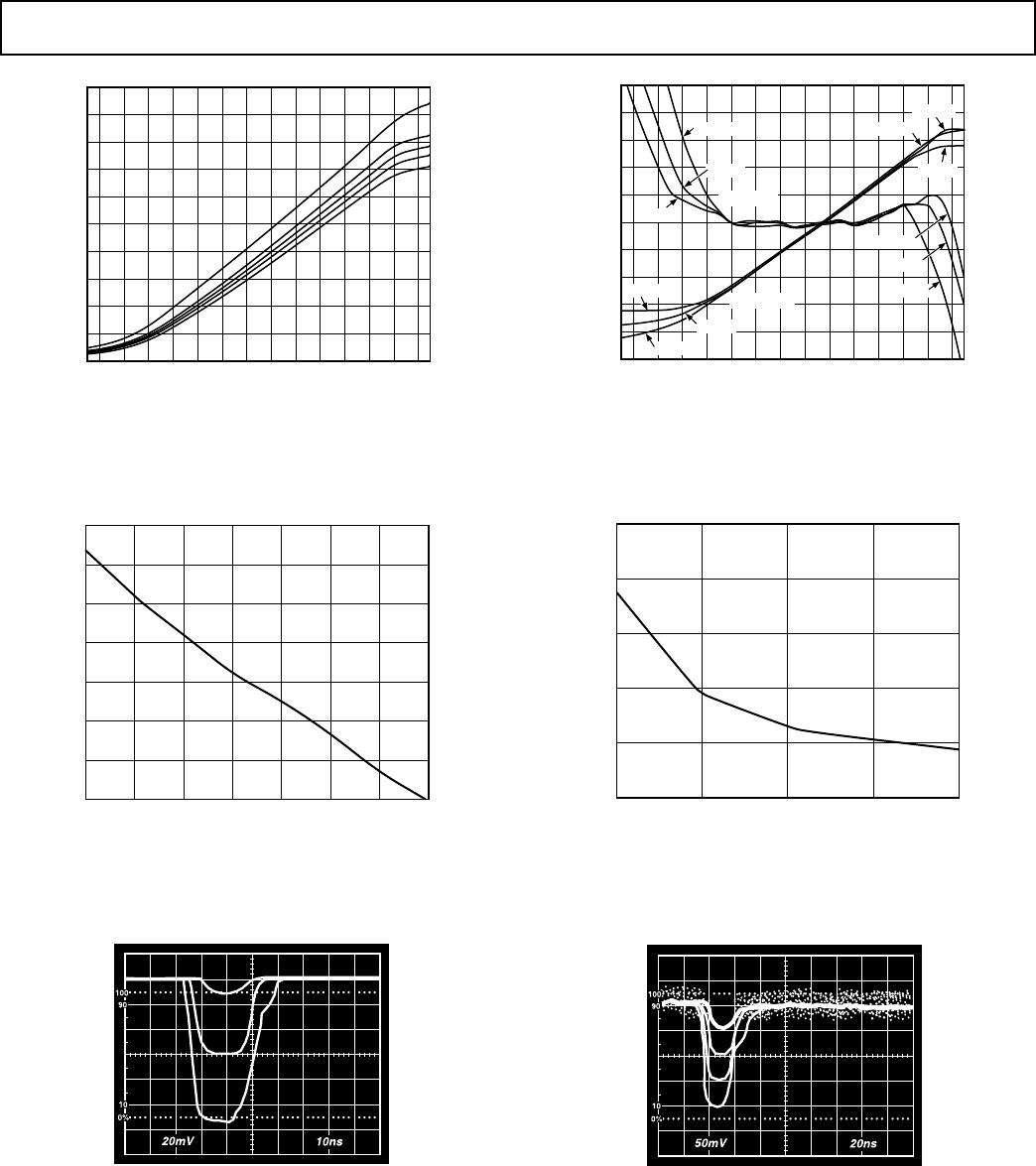
Figure 12. Baseband Pulse Response of Single AD641,
Inputs of 1 mV, 10 mV and 100 mV
ERROR IN – dB
INPUT LEVEL – dBm
–2.00
–1.75
0.50
2–48 –44
–40
–4
–1.00
–0.25
–0.00
0.25
–1.50
–1.25
–0.50
–0.75
OUTPUT – mA
–52 –36 –32 –28 –24 –20 –16 –12 –8 0
+258C
+1258C
–558C
+258C
+1258C
–558C
OUTPUT
+258C
+1258C
–558C
+1258C
ERROR
+258C
–558C
5
4
3
2
1
0
–1
–2
–3
–4
–5
Figure 13. Logarithmic Response and Linearity at
200 MHz, T
A
for T
A
= –55
°
C, +25
°
C, +125
°
C
INPUT FREQUENCY – MHz
1.0
0.95
0.75
50 250150 190 210
0.90
0.85
0.80
SLOPE CURRENT – mA
Figure 14. Slope Current, I
Y
, vs. Input Frequency
10
0%
5µs
5µs
20mV
20mV
100
90
Figure 15. Baseband Pulse Response of Cascaded AD641s
at Inputs of 0.2 mV, 2 mV, 20 mV and 200 mV

AD641ANZ

Mfr. #:
Manufacturer:
Description:
Logarithmic Amplifiers IC 250MHZ DEMOD LGAMP
Lifecycle:
New from this manufacturer.
Delivery:
DHL FedEx Ups TNT EMS
Payment:
T/T Paypal Visa MoneyGram Western Union

Products related to this Datasheet