REV. D
AD641
–15–
FREQUENCY – MHz
3
2.5
–0.5
1 100010 100
2
1.5
1
0.5
0
VOLTS – LOG OUT into 1k
0dBm
–20dBm
–35dBm
–50dBm
Figure 31. Single AD641 RSSI vs. Frequency
Figure 31 shows a plot of RSSI vs. frequency for various input
signal amplitudes. It can be seen that at higher frequencies the
output drops off as explained in the section “Effect of Fre-
quency on Calibration.’’ If the RSSI circuit is to be operated at
a known frequency with limited bandwidth, the compensation
techniques described in that section can be used to enhance
accuracy.
250 MHz RSSI Converter with 58 dB Dynamic Range
For a larger dynamic range two AD641s can be cascaded, as
shown in Figure 32. The low end usefulness of the circuit will
be set by the noise floor of the overall environment that the circuit
sees. This includes all sources of both radiated and conducted
noise. Proper layout to avoid conducted noise and good shield-
ing to minimize radiated noise are essential for good low signal
operation.
FREQUENCY – MHz
4.5
3.5
0
1 100010 100
2
2.5
1
1.5
0.5
VOLTS – LOG OUT into 1k
0dBm
–20dBm
–50dBm
–80dBm
4
3
Figure 33. Cascaded AD641s RSSI vs. Frequency
Filtering between the devices and input offset nulling techniques
described elsewhere are also useful for extending the dynamic
range of two cascaded devices.
Figure 33 shows a plot of this circuit vs. frequency for various
input amplitudes. The drop off at high frequency can be seen to
be greater than for the single device case due to the compound-
ing effects of the bandwidth limiting of the extra stages.
6
7
4
3
U3
AD846
2
–6V
4.7V
LOG
OUTPUT
+50mV/dB
(LO)
+6V
4.7V
L1
(SEE
TEXT)
(SEE TEXT)
R5
1.13kV
C2
47pF
C1
47pF
+6V
68V
R4
100V
–6V
18V
NC
DENOTES A CONNECTION TO THE
GROUND PLANE; OBSERVE COMMON
CONNECTIONS WHERE SHOWN.
ALL UNMARKED CAPACITORS ARE
0.1mF CERAMIC. FOR VALUES OF
NUMBERED COMPONENTS SEE TEXT
R3
100V
NC
NC
R1
R2
SIGNAL
INPUT
9
87
6
10
53214
12
1314
15
11
16181920 17
LOG
OUT
LOG
COM
SIG
+OUT
RG2
–V
S
SIG
–OUT
RG0RG1CKT
COM
ATN
OUT
SIG
+IN
+V
S
ITC
BL1
ATN
IN
ATN
COM
ATN
COM
ATN
LO
SIG
–IN
BL2
1kV
1kV
U1 AD641
9
87
6
10
53214
12
1314
15
11
16181920 17
LOG
OUT
LOG
COM
SIG
+OUT
RG2
–V
S
SIG
–OUT
RG0RG1CKT
COM
ATN
OUT
SIG
+IN
+V
S
ITCBL1
ATN
IN
ATN
COM
ATN
COM
ATN
LO
SIG
–IN
BL2
1kV
1kV
U2 AD641
68V
18V
Figure 32. Complete 58 dB Dynamic Range Converter for 250 MHz Operation
AD641
Rev. D | Page 16
OUTLINE DIMENSIONS
CONTROLLING DIMENSIONS ARE IN INCHES; MILLIMETER DIMENSIONS
(IN PARENTHESES) ARE ROUNDED-OFF INCH EQUIVALENTS FOR
REFERENCE ONLY AND ARE NOT APPROPRIATE FOR USE IN DESIGN.
CORNER LEADS MAY BE CONFIGURED AS WHOLE OR HALF LEADS.
COMPLIANT TO JEDEC STANDARDS MS-001
070706-A
0.022 (0.56)
0.018 (0.46)
0.014 (0.36)
0.150 (3.81)
0.130 (3.30)
0.115 (2.92)
0.070 (1.78)
0.060 (1.52)
0.045 (1.14)
20
1
10
11
0.100 (2.54)
BSC
1.060 (26.92)
1.030 (26.16)
0.980 (24.89)
0.210 (5.33)
MAX
SEATING
PLANE
0.015
(0.38)
MIN
0.005 (0.13)
MIN
0.280 (7.11)
0.250 (6.35)
0.240 (6.10)
0.060 (1.52)
MAX
0.430 (10.92)
MAX
0.014 (0.36)
0.010 (0.25)
0.008 (0.20)
0.325 (8.26)
0.310 (7.87)
0.300 (7.62)
0.015 (0.38)
GAUGE
PLANE
0.195 (4.95)
0.130 (3.30)
0.115 (2.92)
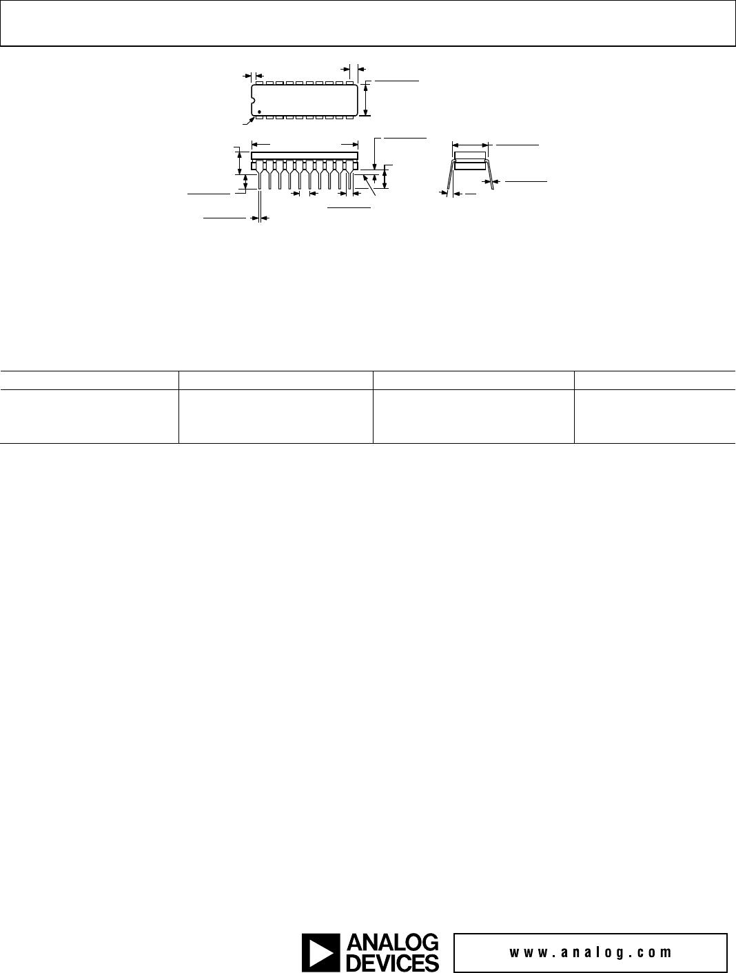
Fig
ure 33. 20-Lead Plastic Dual In-Line Package [PDIP]
Narrow Body
(N-20)
Dimensions shown in inches and (millimeters)
COMPLIANT TO JEDEC STANDARDS MO-047-AA
CONTROLLING DIMENSIONS ARE IN INCHES; MILLIMETER DIMENSIONS
(IN PARENTHESES) ARE ROUNDED-OFF INCH EQUIVALENTS FOR
REFERENCE ONLY AND ARE NOT APPROPRIATE FOR USE IN DESIGN.
0.020 (0.50)
R
BOTTOM
VIEW
(PINS UP)
0.021 (0.53)
0.013 (0.33)
0.330 (8.38)
0.290 (7.37)
0.032 (0.81)
0.026 (0.66)
0.056 (1.42)
0.042 (1.07)
0.20 (0.51)
MIN
0.120 (3.04)
0.090 (2.29)
3
4
19
18
8
9
14
13
TOP VIEW
(PINS DOWN)
0.395 (10.03)
0.385 (9.78)
SQ
0.356 (9.04)
0.350 (8.89)
SQ
0.048 (1.22 )
0.042 (1.07)
0.048 (1.22)
0.042 (1.07)
0.020
(0.51)
R
0.050
(1.27)
BSC
0.180 (4.57)
0.165 (4.19)
0.045 (1.14)
0.025 (0.64)
R
PIN 1
IDENTIFIER
Fig
ure 34. 20-Lead Plastic Leaded Chip Carrier [PLCC]
(P-20)
Dimensions shown in inches and (millimeters)
AD641
Rev. D | Page 17
20
1
10
11
0.310 (7.87)
0.220 (5.59)
PIN 1
0.005
(0.13)
MIN
0.098 (2.49)
MAX
15°
0.320 (8.13)
0.290 (7.37)
0.015 (0.38)
0.008 (0.20)
SEATING
PLANE
0.200 (5.08)
MAX
1.060 (26.92) MAX
0.150 (3.81)
MIN
0.200 (5.08)
0.125 (3.18)
0.023 (0.58)
0.014 (0.36)
0.100
(2.54)
BSC
0.070 (1.78)
0.030 (0.76)
0.060 (1.52)
0.015 (0.38)
CONTROLLING DIMENSIONS ARE IN INCHES; MILLIMETER DIMENSIONS
(IN PARENTHESES) ARE ROUNDED-OFF INCH EQUIVALENTS FOR
REFERENCE ONLY AND ARE NOT APPROPRIATE FOR USE IN DESIGN.
Figure 3
5. 20-Lead Ceramic Dual In-Line Package [CERDIP]
(Q-20)
Dimensions shown in inches and (millimeters)
ORDERING GUIDE
Model
1
Temperature Range Package Description
Package Option
−40°C to +85°C 20-Lead PDIP N-20
−40°C to +85°C 20-Lead PLCC P-20
AD641ANZ
AD641APZ
5962-9559802MRA
−55°C to +125°C 20-Lead CERDIP Q-20
1
Z = RoHS Compliant Part.
©1999–2016 Analog Devices, Inc. All rights reserved. Trademarks and
registered trademarks are the property of their respective owners.
C2014c-0-6/16(D)

AD641ANZ

Mfr. #:
Manufacturer:
Description:
Logarithmic Amplifiers IC 250MHZ DEMOD LGAMP
Lifecycle:
New from this manufacturer.
Delivery:
DHL FedEx Ups TNT EMS
Payment:
T/T Paypal Visa MoneyGram Western Union

Products related to this Datasheet