10
IDT72205LB/72215LB/72225LB/72235LB/72245LB CMOS SyncFIFO
TM
256 x 18, 512 x 18, 1,024 x 18, 2,048 x 18 and 4,096 x 18
COMMERCIAL AND INDUSTRIAL
TEMPERATURE RANGES
MARCH 2013
NOTES:
1. When tSKEW2 minimum specification, tFRL (maximum) = tCLK + tSKEW2. When tSKEW2 < minimum specification, tFRL (maximum) = either 2*tCLK + tSKEW2 or tCLK + tSKEW2.
The Latency Timing applies only at the Empty Boundary (EF = LOW).
2. The first word is available the cycle after EF goes HIGH, always.
Figure 7. First Data Word Latency after Reset with Simultaneous Read and Write
Figure 8. Full Flag Timing
WCLK
D0 - D17
RCLK
Q0 - Q17
t
DS
tSKEW2
t ENS
t
REF
t
A
0
12 3
D
DDD
01
DD
(first valid write)
t
OE
t
OLZ
tA
t
FRL
(1)
D
4
tENS
2766 drw 09
NOTE:
1. tSKEW1 is the minimum time between a rising RCLK edge and a rising WCLK edge to guarantee that FF will go HIGH during the current clock cycle. If the time between the rising
edge of RCLK and the rising edge of WCLK is less than tSKEW1, then FF may not change state until the next WCLK edge.
DATA READ
WCLK
D
0
- D
17
RCLK
Q
0
- Q
17
t
A
t
WFF
DATA WRITE
t
WFF
t
ENH
t
ENS
t
DS
t
WFF
t
DS
DATA
WRITE
NEXT DATA READ
t
A
NO WRITE NO WRITE
DATA IN OUTPUT REGISTER
LOW
t
SKEW1
(1)
t
SKEW1
(1)
t
ENH
t
ENS
2766 drw 10
11
IDT72205LB/72215LB/72225LB/72235LB/72245LB CMOS SyncFIFO
TM
256 x 18, 512 x 18, 1,024 x 18, 2,048 x 18 and 4,096 x 18
COMMERCIAL AND INDUSTRIAL
TEMPERATURE RANGES
MARCH 2013
NOTE:
1. When tSKEW2 minimum specification, tFRL (maximum) = tCLK + tSKEW2. When tSKEW2 < minimum specification, tFRL (maximum) = either 2*tCLK + tSKEW2 or tCLK + tSKEW2.
The Latency Timing applies only at the Empty Boundary (EF = LOW).
Figure 9. Empty Flag Timing
Figure 10. Write Programmable Registers
WCLK
D
0
- D
17
RCLK
Q
0
- Q
17
t
DS
t
ENS
t
A
t
SKEW2
DATA WRITE 1
DATA READ
t
ENH
t
REF
t
DS
t
ENS
DATA WRITE 2
t
ENH
t
REF
DATA IN OUTPUT REGISTER
t
FRL
(1)
LOW
2766 drw 11
t
REF
t
SKEW2
t
FRL
(1)
WCLK
tCLKH tCLKL
tCLK
tENS tENH
LD
WEN
D0–D15
tDS tDH
PAE OFFSET PAF OFFSET
D0–D11
PAE OFFSET
tENS
2766 drw 12
Figure 11. Read Programmable Registers
RCLK
t
CLKH
t
CLKL
t
CLK
t
ENS
t
ENH
Q
0
–Q
15
PAE OFFSET PAF OFFSET
PAE OFFSET
UNKNOWN
t
A
t
ENS
2766 drw 13
12
IDT72205LB/72215LB/72225LB/72235LB/72245LB CMOS SyncFIFO
TM
256 x 18, 512 x 18, 1,024 x 18, 2,048 x 18 and 4,096 x 18
COMMERCIAL AND INDUSTRIAL
TEMPERATURE RANGES
MARCH 2013
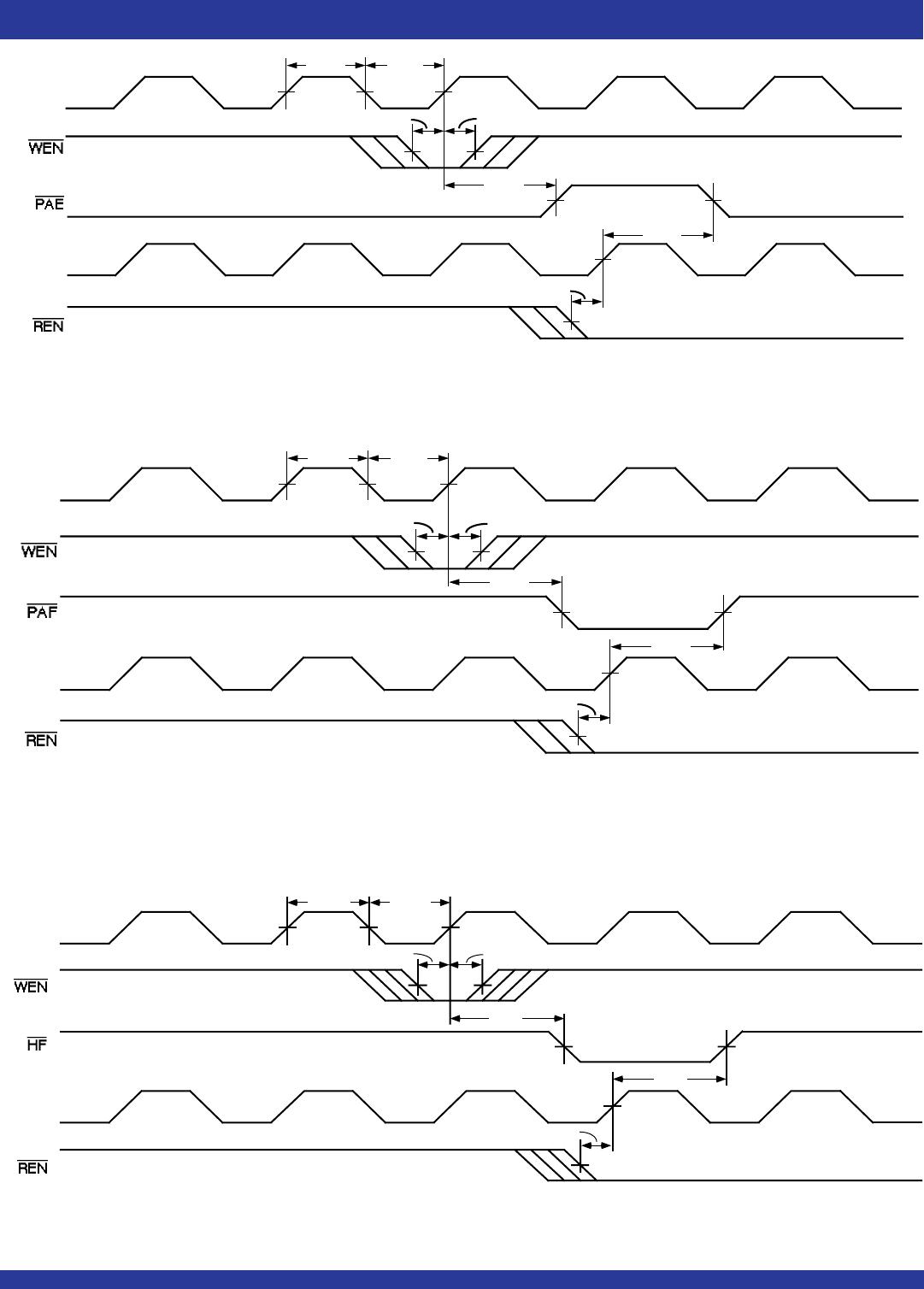
Figure 12. Programmable Almost-Empty Flag Timing
Figure 13. Programmable Almost-Full Flag Timing
WCLK
tCLKH tCLKL
tENS tENH
tENS
tPAE
n + 1 words in FIFO
n words in FIFO
RCLK
tPAE
2766 drw 14
WCLK
tCLKH
tCLKL
tENS
tENH
tENS
tPAF
D – m + 1 words
in FIFO memory
RCLK
tPAF
(1)
2766 drw 15
D – m words
in FIFO memory
(2)
(1)
D – m + 1 words in FIFO memory
(1)
Figure 14. Half-Full Flag Timing
WCLK
t
ENS
t
ENH
t
ENS
t
HF
RCLK
t
HF
D/2 words in
FIFO memory
(1)
2766 drw 16
D/2 + 1 words in
FIFO memory
(2)
D/2 words in FIFO memory
(1)
t
CLKL
t
CLKH
NOTES:
1. D = maximum FIFO Depth =
256 words for the IDT72205LB, 512 words for the IDT72215LB, 1,024 words for the IDT72225LB, 2,048 words for the IDT72235LB and 4,096 words
for the IDT72245LB.
NOTE:
1. n = PAE offset. Number of data words written into FIFO already = n.
NOTES:
1. m = PAF offset. D = maximum FIFO Depth. Number of data words written into FIFO memory
= 256 - m + 1 for the IDT72205LB, 512 - m + 1 for the IDT72215LB,
1,024 - m + 1 for the IDT72225LB, 2,048 - (m + 1) for the IDT72235LB and 4,096 - (m + 1) for the IDT72245LB.
2.
256 - m words for the IDT72205LB, 512 - m words for the IDT72215LB, 1,024 - m words for the IDT72225LB, 2,048 - m words for the IDT72235LB and 4,096 - m words for
the IDT72245LB.

72225LB15TF

Mfr. #:
Manufacturer:
IDT
Description:
FIFO 1K X 18 FIFO SYNCHRONOUS
Lifecycle:
New from this manufacturer.
Delivery:
DHL FedEx Ups TNT EMS
Payment:
T/T Paypal Visa MoneyGram Western Union