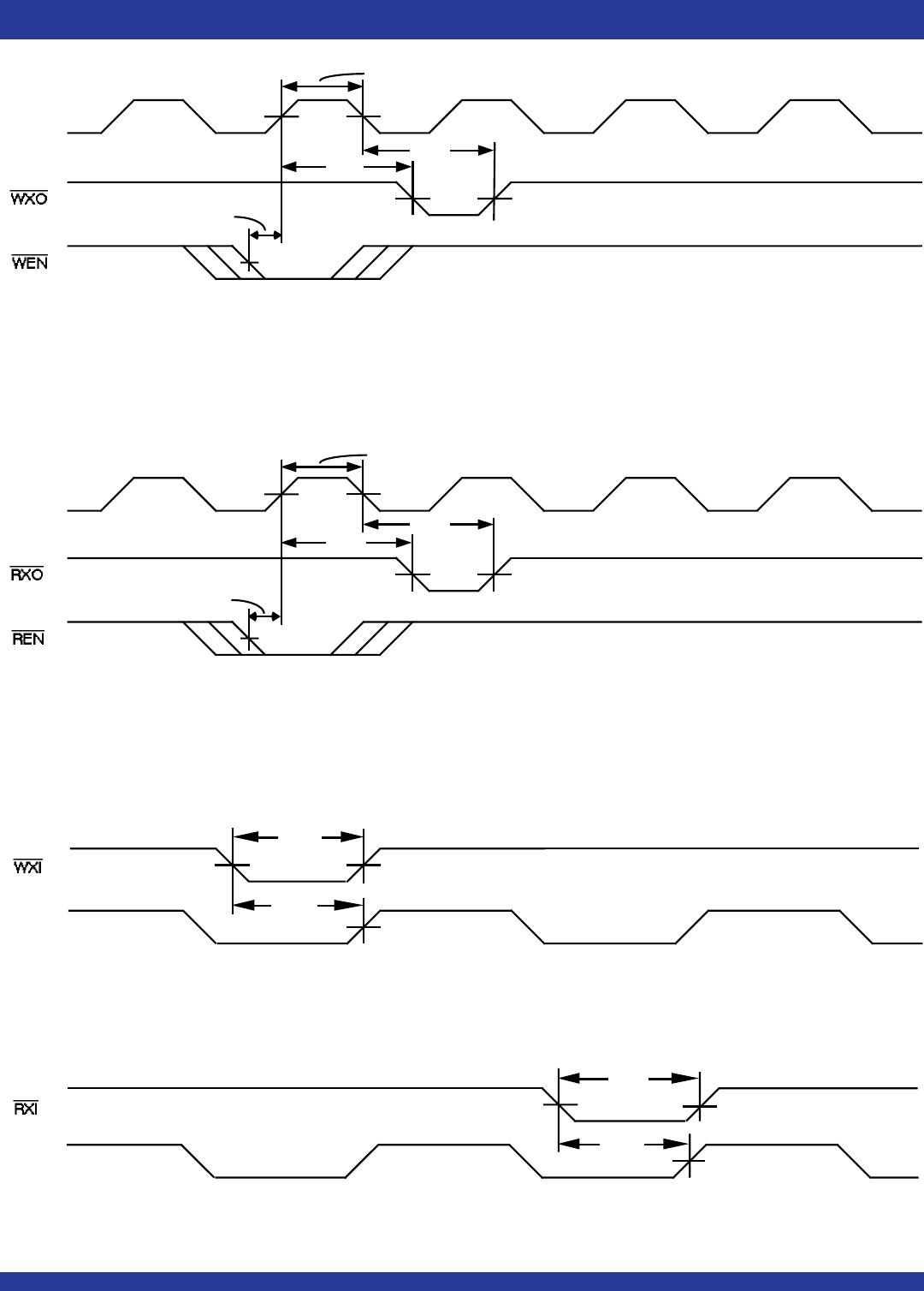
13
IDT72205LB/72215LB/72225LB/72235LB/72245LB CMOS SyncFIFO
TM
256 x 18, 512 x 18, 1,024 x 18, 2,048 x 18 and 4,096 x 18
COMMERCIAL AND INDUSTRIAL
TEMPERATURE RANGES
MARCH 2013
WCLK
t
ENS
t CLKH
tXO
Note 1
tXO
2766 drw 17
NOTE:
1. Write to Last Physical Location.
Figure 18. Read Expansion In Timing
RCLK
t ENS
t CLKH
tXO
Note 1
tXO
2766 drw 18
RCLK
t
t
XI
XIS
2766 drw 20
NOTE:
1. Read from Last Physical Location.
Figure 16. Read Expansion Out Timing
Figure 15. Write Expansion Out Timing
Figure 17. Write Expansion In Timing
WCLK
t XI
t XIS
2766 drw 19
14
IDT72205LB/72215LB/72225LB/72235LB/72245LB CMOS SyncFIFO
TM
256 x 18, 512 x 18, 1,024 x 18, 2,048 x 18 and 4,096 x 18
COMMERCIAL AND INDUSTRIAL
TEMPERATURE RANGES
MARCH 2013
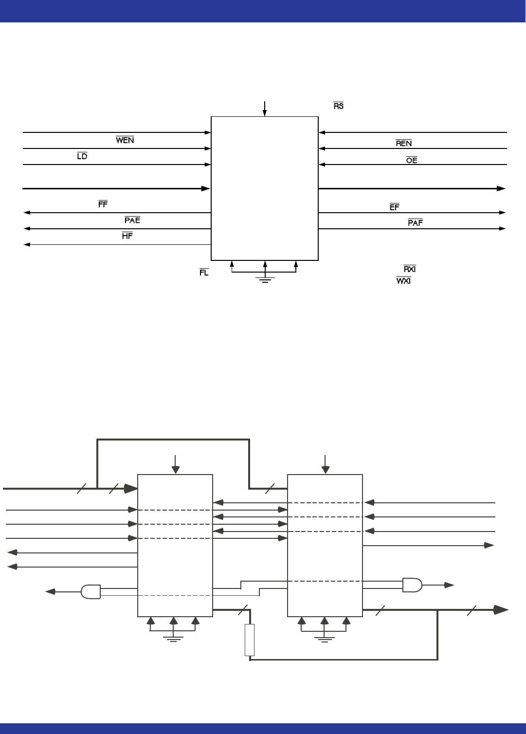
OPERATING CONFIGURATIONS
SINGLE DEVICE CONFIGURATION
A single IDT
72205LB/72215LB/72225LB/72235LB/72245LB may be used
when the application requirements are for 256/512/1,024/2,048/4,096 words
or less. These FIFOs are in a single Device Configuration when the First Load
(FL), Write Expansion In (WXI) and Read Expansion In (RXI) control inputs
are grounded (Figure 19).
Figure 19. Block Diagram of Single 256 x 18, 512 x 18, 1,024 x 18, 2,048 x 18, 4,096 x 18 Synchronous FIFO
NOTE:
1. Do not connect any output control signals directly together.
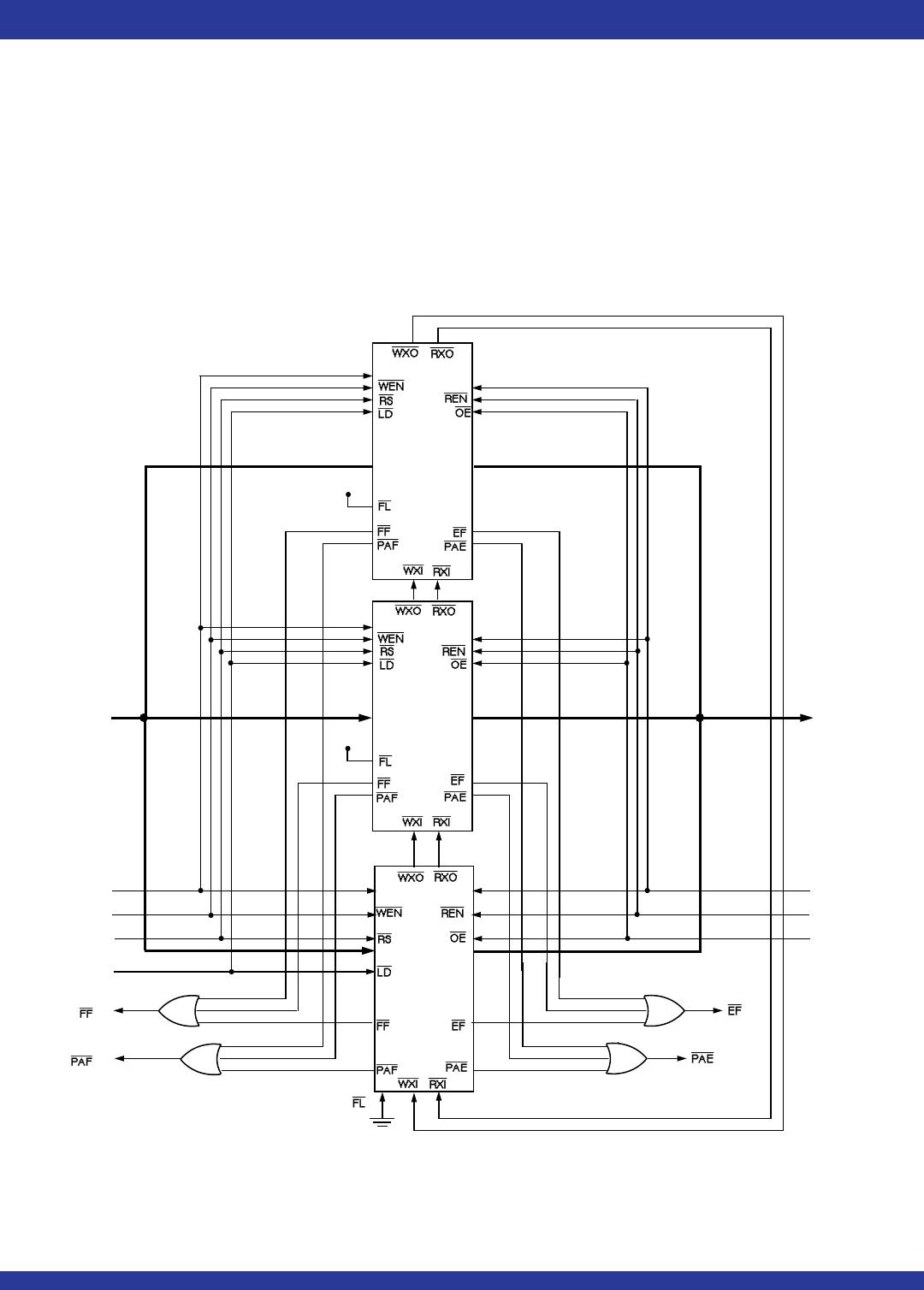
Figure 20. Block Diagram of 256 x 36, 512 x 36, 1,024 x 36, 2,048 x 36, 4,096 x 36
Synchronous FIFO Memory Used in a Width Expansion Configuration
WIDTH EXPANSION CONFIGURATION
Word width may be increased simply by connecting together the control
signals of multiple devices. Status flags can be detected from any one device.
The exceptions are the Empty Flag and Full Flag. Because of variations in skew
between RCLK and WCLK, it is possible for flag assertion and deassertion to
vary by one cycle between FIFOs. To avoid problems the user must create
composite flags by ANDing the Empty Flags of every FIFO, and separately
ANDing all Full Flags. Figure 20 demonstrates a 36-word width by using two
IDT72205LB/72215LB/72225LB/72235LB/72245LBs. Any word width can
be attained by adding additional IDT72205LB/72215LB/72225LB/72235LB/
72245LBs. Please see the Application Note AN-83.
WRITE CLOCK (WCLK)
WRITE ENABLE (WEN)
READ CLOCK (RCLK)
READ ENABLE (REN)
LOAD (LD)
OUTPUT ENABLE (OE)
DATA IN (D)
DATA OUT (Q)
FULL FLAG (FF)
PROGRAMMABLE (PAE)
HALF FULL FLAG (HF)
EMPTY FLAG (EF)
PROGRAMMABLE (PAF)
RESET (RS)
72205LB
72215LB
72225LB
72235LB
72245LB
72205LB
72215LB
72225LB
72235LB
72245LB
RESET (RS)
36
36
18 18
18
18
FF FF EFEF
2766 drw 22
FIRST LOAD (FL)
READ EXPANSION IN (RXI)
WRITE EXPANSION IN (WXI)
WRITE CLOCK (WCLK)
WRITE ENABLE (
)
READ CLOCK (RCLK)
READ ENABLE (
)
LOAD (
)
OUTPUT ENABLE (
)
DATA IN (D
0
- D
17
)
DATA OUT (Q
0
- Q
17
)
FULL FLAG (
)
PROGRAMMABLE (
)
HALF-FULL FLAG (
)
EMPTY FLAG (
)
PROGRAMMABLE (
)
RESET (
)
IDT
72205LB
72215LB
72225LB
72235LB
72245LB
2766 drw 21
FIRST LOAD ( )
READ EXPANSION IN (
)
WRITE EXPANSION IN (
)
15
IDT72205LB/72215LB/72225LB/72235LB/72245LB CMOS SyncFIFO
TM
256 x 18, 512 x 18, 1,024 x 18, 2,048 x 18 and 4,096 x 18
COMMERCIAL AND INDUSTRIAL
TEMPERATURE RANGES
MARCH 2013
Figure 21. Block Diagram of 768 x 18, 1,536 x 18, 3,072 x 18, 6,144 x 18, 12,288 x 18 Synchronous
FIFO Memory With Programmable Flags used in Depth Expansion Configuration
LOAD
WRITE CLOCK
WRITE ENABLE
READ CLOCK
READ ENABLE
OUTPUT ENABLE
DATA IN
DATA OUT
RESET
IDT
72205LB
72215LB
72225LB
72235LB
72245LB
FIRST LOAD ( )
Vcc
Vcc
IDT
72205LB
72215LB
72225LB
72235LB
72245LB
IDT
72205LB
72215LB
72225LB
72235LB
72245LB
2766 drw 23
RCLK
WCLK
RCLK
WCLK
RCLK
WCLK
Dn
Qn
Dn
Qn
Dn
Qn
DEPTH EXPANSION CONFIGURATION —
(WITH PROGRAMMABLE FLAGS)
These devices can easily be adapted to applications requiring more than 256/
512/1,024/2,048/4,096 words of buffering. Figure 21 shows Depth Expansion
using three IDT72205LB/72215LB/72225LB/72235LB/72245LBs. Maximum
depth is limited only by signal loading. Follow these steps:
1. The first device must be designated by grounding the First Load (FL)
control input.
2. All other devices must have FL in the HIGH state.
3. The Write Expansion Out (WXO) pin of each device must be tied to
the Write Expansion In (WXI) pin of the next device. See Figure 21.
4.The Read Expansion Out (RXO) pin of each device must be tied to the
Read Expansion In (RXI) pin of the next device. See Figure 21.
5.All Load (LD) pins are tied together.
6.The Half-Full Flag (HF) is not available in this Depth Expansion
Configuration.
7. EF, FF, PAE, and PAF are created with composite flags by ORing
together every respective flags for monitoring. The composite PAE
and PAF flags are not precise.

72225LB15TF

Mfr. #:
Manufacturer:
IDT
Description:
FIFO 1K X 18 FIFO SYNCHRONOUS
Lifecycle:
New from this manufacturer.
Delivery:
DHL FedEx Ups TNT EMS
Payment:
T/T Paypal Visa MoneyGram Western Union