BD8153EFV
Technical Note
4/17
www.rohm.com
2009.07 - Rev.B
© 2009 ROHM Co., Ltd. All rights reserved.
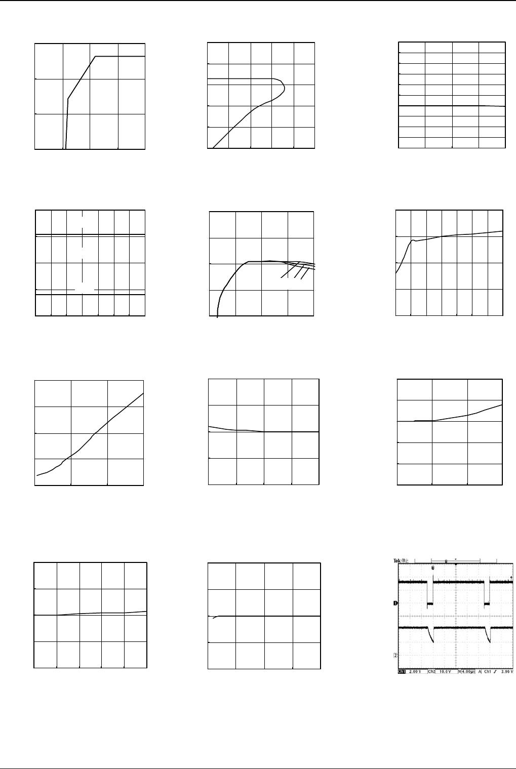
OUTPUT VOLTAGE : Vcp[mV].
0
40
80
120
160
200
0 20 40 60 80 100
INPUT CURRENT : Icp[mA]
1.22
1.23
1.24
1.25
1.26
-50 -25 0 25 50 75 100 125
AMBIENT TEMPERATURE : Ta[
]
REF VOLTAGE : VREF[V
]
0
2
4
6
8
10
01.534.56
SUPPLY VOLTAGE : VDD[V]
SUPPLY CURRENT : IDD[mA]
0
0.2
0.4
0.6
0.8
1
0 1.5 3 4.5 6
SUPPLY VOLTAGE : VCC [V]
SUPPLY CURRENT : ICC[mA]
125
25
-40
Fig. 10 SW On Resistance
0
40
80
120
160
200
0 0.2 0.4 0.6 0.8 1
SW CURRENT : ISW [A]
SW VOLTAGE : VSW [V]
Fig. 12 Gate Shading
On Voltage
GS CURRENT : Igs[mA]
GS VOLTAGE : Vgs[V]
Fig. 11 Charge Pump
On Voltage
N channel
P channel
Fig. 4 Internal
Reference Line Regulation
0
0.4
0.8
1.2
1.6
01.534.56
SUPPLY VOLTAGE : VCC[V]
REF VOLTAGE : VREF[V]
Fig. 5 Internal
Reference Load Regulation
0
0.4
0.8
1.2
1.6
0 5 10 15 20 25 30
REF CURRENT : IREF[mA]
REF VOLTAGE : VREF[V]
Fig. 6 SS Source Current
0
2
4
6
8
10
12
01.534.56
SUPPLY VOLTAGE : VDD[V]
SS SOURCE CURRENT : ISS[μA]
.
Fig. 7 DLS Source Current
0
2
4
6
8
10
12
01.534.56
SUPPLY VOLTAGE : VDD[V]
DLS SOURCE CURRENT : IDLS[μA]
Fig. 8 Switching Frequency
Temperature
0
0.5
1
1.5
2
-50 -25 0 25 50 75 100 125
AMBIENT TEMPERATURE : Ta[
]
SWITCHHING FREQUENCY : f [MHz]
-40
Fig. 9 REG Current Capacity
0
1
2
3
4
5
0246810
BASE CURRENT : IBASE[mA]
VDD VOLTAGE : VDD[V]
Fig. 1 Total Supply Current 1
Fig. 3 Internal Reference
Temperature
Fig. 2 Total Supply Current 2
125
25
-40
N channel
P channel
0
20 40 60 80 100
0
0.2
0.4
0.6
0.8
1
Reference Data (Unless otherwise specified, Ta = 25°C)
BD8153EFV
Technical Note
5/17
www.rohm.com
2009.07 - Rev.B
© 2009 ROHM Co., Ltd. All rights reserved.
Reference Data (Unless otherwise specified, Ta = 25°C)
0
1
2
3
4
5
00.40.81.21.62
OUTPUT CURRENT : IDD[mA]
OUTPUT VOLTAGE : VDD[V]
11.5
11.6
11.7
11.8
11.9
12.0
12.1
12.2
12.3
12.4
12.5
23456
SUPPLY VOLTAGE : VCC[V]
Vo1 VOLTAGE : VO1[V]
Fig. 16 Vo1 Load Regulation
10
11
12
13
14
0 100 200 300 400 500 600 700
OUTPUT CURRENT : IO[mA]
OUTPUT VOLTAGE : VO1[V]
13V
12V
10.8V
Fig. 14 VDD Load Regulation
Fig. 15 Vo1 Line Regulation
Fig. 19 Power Supply Voltage vs
Max. Output Current Capacity
0
400
800
1200
1600
1.534.56
SUPPLY VOLTAGE : VCC[V]
MAXIMUM CURRENT : IoMAX[mA]
Fig. 20 Vo2 Line Regulation
23.4
23.5
23.6
23.7
23.8
10 11.5 13 14.5 16
INPUT VOLTAGE : Vo1[v]
OUTPUT VOLTAGE : VO2[V]
Fig. 21 Vo2 Load Regulation
23
23.2
23.4
23.6
23.8
24
0 50 100 150
OUTPUT CURRENT : IO2[mA]
OUTPUT VOLTAGE : VO2[V]
Fig. 22 Negative-side Charge
Pump Line Regulation
-6.4
-6.3
-6.2
-6.1
-6
10 11 12 13 14 15
INPUT VOLTAGE : VO1[V]
OUTPUT VOLTAGE : VO3[V]
Fig. 23 Negative-side Charge
Pump Load Regulation
-6.4
-6.3
-6.2
-6.1
-6
0 50 100 150 200
OUTPUT CURRENT : IO[mA]
OUTPUT VOLTAGE : VO1[V]
Fig. 13 Vo1 Line Regulation
0
5
10
15
0 1.5 3 4.5 6
SUPPLY VOLTAGE : VCC [V]
OUTPUT VOLTAGE : VDD [V]
Fig. 17 Efficiency vs Output Current
60
70
80
90
100
2.5 3 3.5 4 4.5 5 5.5 6
SUPPLY VOLTAGE : VCC[V]
EFFICIENCY [ % ]
Fig. 18 Efficiency vs Power
Supply Voltage
Fig. 24 Gate Shading
Output Waveform
IG
VO2GS
80
85
90
95
100
0 150 300 450 600
OUTPUT CURRENT : IO1[mA]
EFFICIENCY [ % ]
10.8V 12V 13V
BD8153EFV
Technical Note
6/17
www.rohm.com
2009.07 - Rev.B
© 2009 ROHM Co., Ltd. All rights reserved.
Pin Assignments Diagram Block Diagram
Fig. 25 Pin Arrangements and Block Diagram
Pin Assignments and Function
PIN
NO.
Pin
name
Function
PIN
NO.
Pin
name
Function
1 GND Ground pin 13 Vo2 Positive-side charge pump output
2 VDD LDO feedback input pin 14 Vo2GS Gate shading source output pin
3 BASE LDO base drive output pin 15 GSOUT Gate shading sink output pin
4 VCC Power supply input pin 16 C2H Flying capacitor connection pin
5 DLS Capacity connection pin for delay start 17 C2L Flying capacitor connection pin
6 COMP DC/DC difference amplifier output 18 C1L Flying capacitor connection pin
7 FB1 DC/DC feedback input 19 C1H Flying capacitor connection pin
8 SS Soft start capacitor connection pin 20 Vo1 Negative-side charge pump power supply input pin
9 PGND Ground pin 21 C3 Negative-side charge pump driver output
10 SW Switch output 22 GND Ground pin
11 IG Gate shading input 23 FB3 Negative-side charge pump feedback input
12 FB2 Positive-side charge pump feedback input 24 REF Internal standard output pin
GND
VDD
BASE
VCC
DLS
COMP
FB1
SS
PGND
SW
IG
FB2
REF
FB3
GND
C3
Vo1
C1H
C1L
C2L
GSOUT
Vo2GS
Vo2
C2H
1uF
4.7uF
VDD=3.3V
IG
Vo2 23.5V
(
30V MAX
)
Vo1=14.5V
(
18V MAX
)
VCC
5V
VREF
Step-up
TSD
UVLO
Charge
Pump
Control 1
Regulator
Ctl
Charge
Pump
Control 2
10uF
10uF
10uF
160k
Ω
15k
Ω
0.1uF
0.1uF
5.1k
Ω
1000
p
F
Vcc
0.1uF
1uF
91k
Ω
18k
Ω
0.1uF
270k
Ω
16k
Ω
0.1uF
1uF
Vo1
Vo1
SS
REF
COMP
VCC
GND
GND
SW
Vo1
FB1
Vo2
C2H
C2L
C1H
C1
L
FB2
C3
FB3
REF
DLS
VCC
0.1uF
Start-up
Controller
PGND
DET2
1.1V
1.1V
DET4
Gate
Shading
Controller
R
Vo2G
GSOUT
0.01uF
Vo2G
DET3
0.3V
Vo1
DET1
1.8V
PGND
BASE
Vo3=-5V
VDD
DET2
DET4
Controller

BD8153EFV-E2

Mfr. #:
Manufacturer:
Description:
LCD Drivers 4-CHANNEL SYST POWER 5V INPUT
Lifecycle:
New from this manufacturer.
Delivery:
DHL FedEx Ups TNT EMS
Payment:
T/T Paypal Visa MoneyGram Western Union

Products related to this Datasheet