BD8153EFV
Technical Note
7/17
www.rohm.com
2009.07 - Rev.B
© 2009 ROHM Co., Ltd. All rights reserved.
Fig. 26 Starting Timing Chart
Block Function
Step-up Controller
A controller circuit for DC/DC boosting.
The switching duty is controlled so that the feedback voltage FB1 is set to 1.24 V (typ.).
A soft start operates at the time of starting. Therefore, the switching duty is controlled by the SS pin voltage.
Charge Pump Control 1
A controller circuit for the positive-side charge pump.
The switching amplitude is controlled so that the feedback voltage FB2 will be set to 1.24 V (typ.).
The start delay time can be set in the DLS terminal at the time of starting.
When the DLS voltage reaches 0.6 V (Typ.), switching waves will be output from the C1L and C2L pins.
Charge Pump Control 2
A controller circuit for the negative-side charge pump.
The switching amplitude is controlled so that the feedback voltage FB2 will be set to 0.6 V (Typ.).
Gate Shading Controller
A controller circuit of gate shading.
The Vo2GS and GSOUT are in on/off control according to IG pin input.
Regulator Control
A regulator controller circuit for V
DD voltage generation.
The base pin current is controlled so that VDD voltage will be set to 3.3 V (typ.).
DET 1 to DET 4
A detection circuit of each output voltage. This detected signal is used for the starting sequential circuit.
Start-up Controller
A control circuit for the starting sequence.
Controls to start in order of V
CC VDD Vo1 Vo3 Vo2.
VREF
A block that generates internal reference voltage. 1.24V (Typ.) is output.
TSD/UVLO
Thermal shutdown/Under-voltage lockout protection/circuit blocks.
The thermal shutdown circuit is shut down at an IC internal temperature of 175°C and reset at 160°C.
The under-voltage lockout protection circuit shuts down the IC when the VCC is 1.8 V (typ.) or below.
Starting sequence
For malfunction prevention, starting logic control operates so that each output will rise in order of V
CC VDD Vo1 Vo3 Vo2.
As shown below, detectors DET1 to DET3 detect that the output on the detection side has reached 90% (typ.) of the set voltage,
and starts the next block.
Starting sequence model
VDD
Reg
DET1
CTL1
Step up
DC/DC
Vo1
DET2 CTL2
Negative
Charge
Pump
Vo3
DET3 CTL3
Positive
Charge
Pump
Vo2
VCC
DET4 CLT4
5V
3.3V
Vcc
VDD
Vo2
Vo1
Vo3
0
0
0
BD8153EFV
Technical Note
8/17
www.rohm.com
2009.07 - Rev.B
© 2009 ROHM Co., Ltd. All rights reserved.
Selecting Application Components
(1) Setting the Output L Constant
The coil to use for output is decided by the rating current I
LR and input current maximum value IINMAX of the coil.
Adjust so that I
INMAX +IL does not reach the rating current value ILR. At this time, IL can be obtained by the following equation.
ΔI
L =
1
VCC
Vo-VCC
1
L VCC f
Set with sufficient margin because the coil value may have the dispersion of 30%. If the coil current exceeds the rating
current I
LR of the coil, it may damage the IC internal element.
BD8153EFV uses the current mode DC/DC converter control and has the optimized design at the coil value. A coil
inductance (L) of 4.7 µH to 15 µH is recommended from viewpoints of electric power efficiency, response, and stability.
(2) Output Capacity Settings
For the capacitor to use for the output, select the capacitor which has the larger value in the ripple voltage V
PP
allowance value and the drop voltage allowance value at the time of sudden load change. Output ripple voltage is
decided by the following equation.
ΔV
PP = ILMAX RESR +
1
VCC
(ILMAX -
ΔI
L
)
fCo Vo 2
Perform setting so that the voltage is within the allowable ripple voltage range.
For the drop voltage during sudden load change; V
DR, please perform the rough calculation by the following equation.
VDR =
ΔI
10 us [V]
Co
However, 10 µs is the rough calculation value of the DC/DC response speed. Please set the capacitance considering
the sufficient margin so that these two values are within the standard value range.
(3) Selecting the Input Capacitor
Since the peak current flows between the input and output at the DC/DC converter, a capacitor is required to install at
the input side. For the reason, the low ESR capacitor is recommended as an input capacitor which has the value more
than 10 µF and less than 100 m. If a capacitor out of this range is selected, the excessive ripple voltage is superposed
on the input voltage, accordingly it may cause the malfunction of IC.
However these conditions may vary according to the load current, input voltage, output voltage, inductance and
switching frequency. Be sure to perform the margin check using the actual product.
[A] Here, f is the switching frequency.
[V] Here, f is the switching frequency.
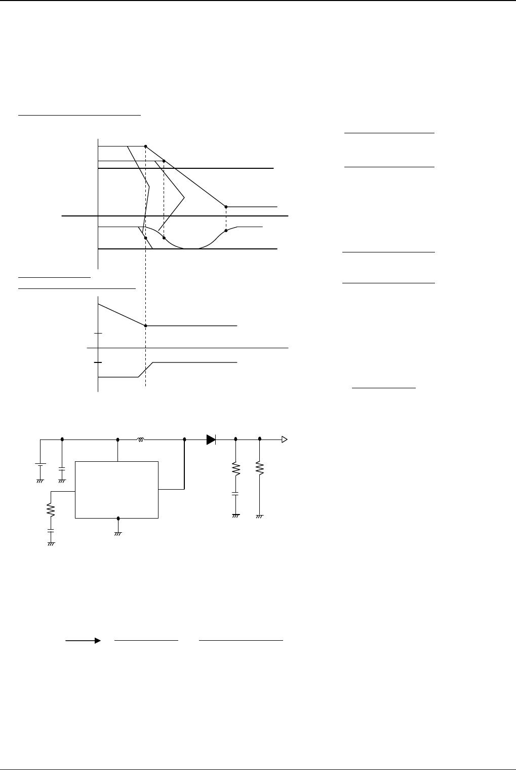
Fig. 27 Coil Current Waveform
Fig. 28 Output Application Circuit Diagram
L
VCC
I
L
Vo
Co
IL
IINMAX + IL should not reach
the rating value level
ILR
IINMAX
average current
BD8153EFV
Technical Note
9/17
www.rohm.com
2009.07 - Rev.B
© 2009 ROHM Co., Ltd. All rights reserved.
(4) Setting RC, CC of the Phase Compensation Circuit
In the current mode control, since the coil current is controlled, a pole (phase lag) made by the CR filter composed of the
output capacitor and load resistor will be created in the low frequency range, and a zero (phase lead) by the output
capacitor and ESR of capacitor will be created in the high frequency range. In this case, to cancel the pole of the power
amplifier, it is easy to compensate by adding the zero point with C
C and RC to the output from the error amp as shown in
the illustration.
Open loop gain characteristics
Pole at the power amplification stage
When the output current reduces, the load resistance
R
o increases and the pole frequency lowers.
Error amp phase
compensation characteristics
Zero at the power amplification stage
When the output capacitor is set larger, the pole
frequency lowers but the zero frequency will not
change. (This is because the capacitor ESR
becomes 1/2 when the capacitor becomes 2 times.)
It is possible to realize the stable feedback loop by canceling the pole fp(Min.), which is created by the output capacitor
and load resistor, with CR zero compensation of the error amp as shown below.
fz(Amp.) = fp(Min.)
1
=
1
2
Rc Cc 2
Romax
Co
1
Fp =
2
R
O
C
O
1
fz(ESR) =
2
E
SR
C
O
1
fp(Min) =
2
R
OMax
C
O
[Hz] at light load
1
fz(Max) =
2
R
OMin
C
O
[Hz] at heavy load
1
fp(Amp.) =
2 R
c
C
c
fp(Min)
fp(Max)
fz(ESR)
A
0
-90
0
Gain
[dB]
Phase
[deg]
l
OUT
Min
l
OUT
Max
0
0
A
-90
Gain
[dB]
Phase
[deg]
L
V
CC
Rc
Cc
Cin
Vcc,PVcc
GND,PGND
SW
COMP
Co
ESR
Ro
Vo
Fig. 29 Gain vs Phase
Fig. 30 Application Circuit Diagram
[Hz]
[Hz]
[Hz]
[Hz]

BD8153EFV-E2

Mfr. #:
Manufacturer:
Description:
LCD Drivers 4-CHANNEL SYST POWER 5V INPUT
Lifecycle:
New from this manufacturer.
Delivery:
DHL FedEx Ups TNT EMS
Payment:
T/T Paypal Visa MoneyGram Western Union

Products related to this Datasheet