CY15B064J
Document Number: 002-10221 Rev. *B Page 10 of 17
AC Test Conditions
Input pulse levels .................................10% and 90% of V
DD
Input rise and fall times .................................................10 ns
Input and output timing reference levels ................0.5 × V
DD
Output load capacitance ............................................ 100 pF
Data Retention and Endurance
Parameter Description Test condition Min Max Unit
T
DR
Data retention T
A
= 85 C10Years
T
A
= 75 C38
T
A
= 65 C 151
NV
C
Endurance Over operating temperature 10
14
Cycles
Capacitance
Parameter
[5]
Description Test Conditions Max Unit
C
O
Output pin capacitance (SDA) T
A
= 25 C, f = 1 MHz, V
DD
= V
DD
(typ) 8 pF
C
I
Input pin capacitance 6pF
Thermal Resistance
Parameter
[5]
Description Test Conditions 8-pin SOIC Unit
JA
Thermal resistance
(junction to ambient)
Test conditions follow standard test methods and proce-
dures for measuring thermal impedance, per
EIA/JESD51.
147 C/W
JC
Thermal resistance
(junction to case)
47 C/W
AC Test Loads and Waveforms
Figure 12. AC Test Loads and Waveforms
3.6 V
OUTPUT
100 pF
1.1 k
Note
5. This parameter is periodically sampled and not 100% tested.
CY15B064J
Document Number: 002-10221 Rev. *B Page 11 of 17
AC Switching Characteristics
Over the Operating Range
Parameter
[6]
Alt.
Parameter
Description Min Max Min Max Min Max Unit
f
SCL
[7]
SCL clock frequency 0.1 0.4 1.0 MHz
t
SU; STA
Start condition setup for repeated Start 4.7 0.6 0.25 s
t
HD;STA
Start condition hold time 4.0 0.6 0.25 s
t
LOW
Clock LOW period 4.7 1.3 0.6 s
t
HIGH
Clock HIGH period 4.0 0.6 0.4 s
t
SU;DAT
t
SU;DATA
Data in setup 250 100 100 ns
t
HD;DAT
t
HD;DATA
Data in hold 0 0 0 ns
t
DH
Data output hold (from SCL @ V
IL
) 0 0 0 ns
t
R
[8]
t
r
Input rise time 1000 300 300 ns
t
F
[8]
t
f
Input fall time 300 300 100 ns
t
SU;STO
STOP condition setup 4.0 0.6 0.25 s
t
AA
t
VD;DATA
SCL LOW to SDA Data Out Valid 3 0.9 0.55 s
t
BUF
Bus free before new transmission 4.7 1.3 0.5 s
t
SP
Noise suppression time constant on SCL, SDA 50 50 50 ns
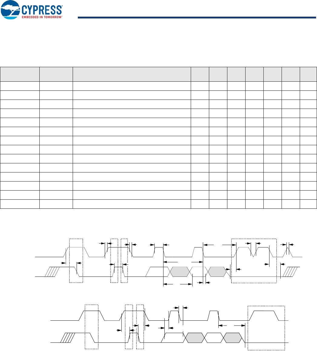
Figure 13. Read Bus Timing Diagram
Figure 14. Write Bus Timing Diagram
t
SU:STA
Start
t
R
t
F
Stop Start
t
BUF
t
HIGH
1/fSCL
t
LOW
t
SP
t
SP
Acknowledge
t
HD:DAT
t
SU:DAT
t
AA
t
DH
SCL
SDA
t
SU:STO
Start
Stop Start Acknowledge
t
AA
t
HD:DAT
t
HD:STA
SCL
SDA
t
SU:DAT
Notes
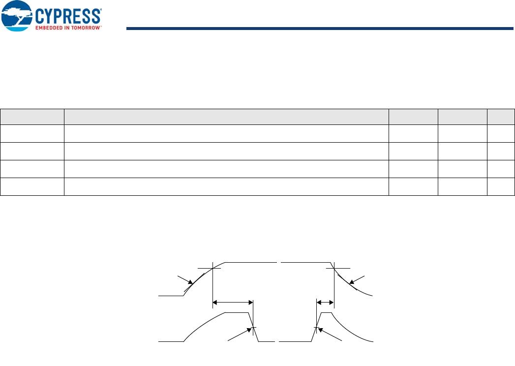
6. Test conditions assume signal transition time of 10 ns or less, timing reference levels of V
DD
/2, input pulse levels of 0 to V
DD
(typ), and output loading of the specified
I
OL
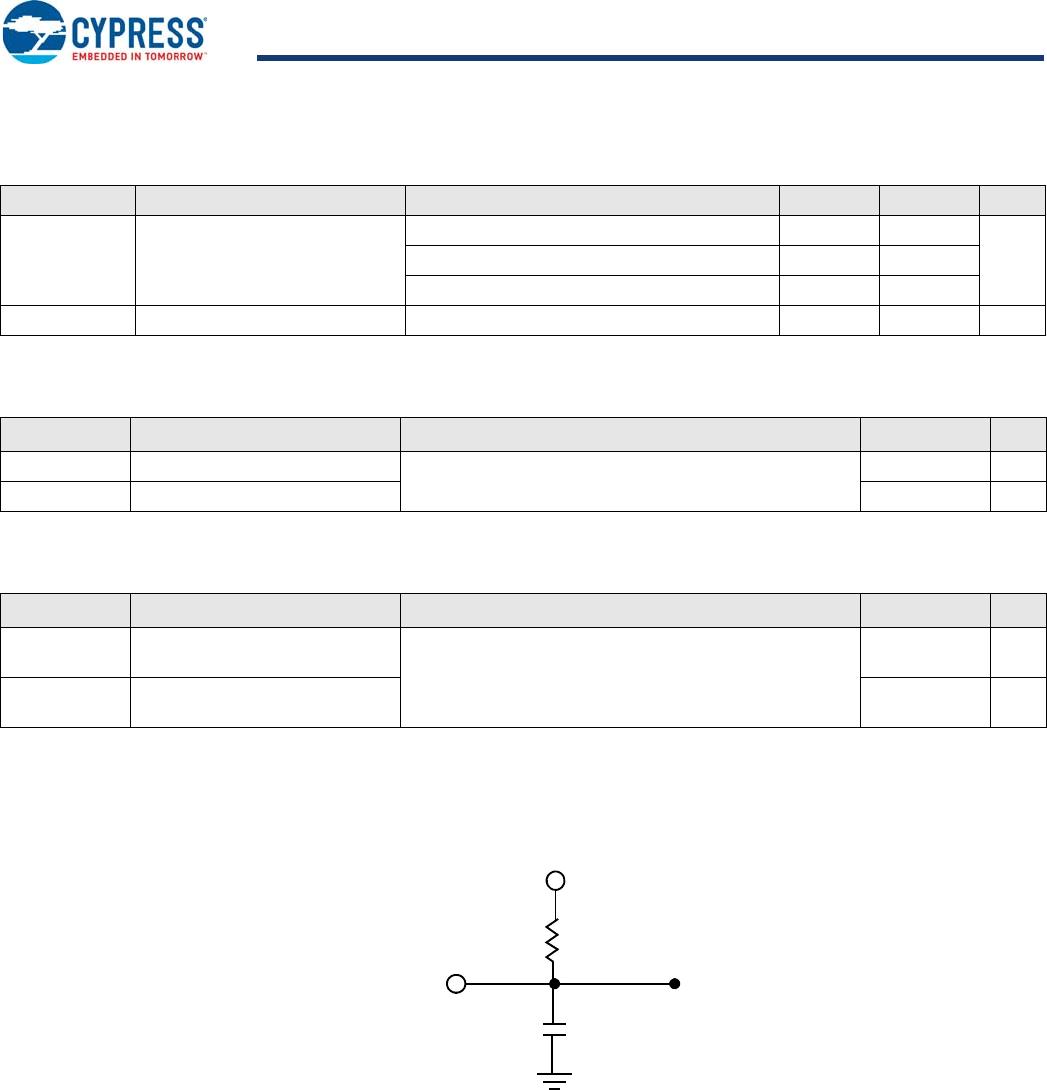
and load capacitance shown in Figure 12.
7. The speed-related specifications are guaranteed characteristic points along a continuous curve of operation from DC to f
SCL
(max).
8. These parameters are guaranteed by design and are not tested.
CY15B064J
Document Number: 002-10221 Rev. *B Page 12 of 17
Power Cycle Timing
Over the Operating Range
Parameter Description Min Max Unit
t
PU
Power-up V
DD
(min) to first access (START condition) 1 ms
t
PD
Last access (STOP condition) to power-down (V
DD
(min)) 0 µs
t
VR
[9, 10]
V
DD
power-up ramp rate 30 µs/V
t
VF
[9, 10]
V
DD
power-down ramp rate 30 µs/V
Figure 15. Power Cycle Timing
SDA
~
~
~
~
t
PU
t
VR t
VF
V
DD
V
DD(min)
t
PD
V
DD(min)
I C START
2
I C STOP
2
Note
9. Slope measured at any point on the V
DD
waveform.
10. Guaranteed by design.

CY15B064J-SXA

Mfr. #:
Manufacturer:
Cypress Semiconductor
Description:
F-RAM F-RAM Memory Serial
Lifecycle:
New from this manufacturer.
Delivery:
DHL FedEx Ups TNT EMS
Payment:
T/T Paypal Visa MoneyGram Western Union

Products related to this Datasheet