AD7894
–9–REV. 0
CONVST, the AD7894 will continue to operate correctly
with the output shift register being reset on the falling edge of
CONVST. However, the SCLK line must be low when CONVST
goes low in order to reset the output shift register correctly.
The serial clock input does not have to be continuous during the
serial read operation. The 16 bits of data (two leading zeros and
14-bit conversion result) can be read from the AD7894 in a
number of bytes.
The AD7894 counts the serial clock edges to know which bit
from the output register should be placed on the SDATA out-
put. To ensure that the part does not lose synchronization, the
serial clock counter is reset on the falling edge of the CONVST
input provided the SCLK line is low. The user should ensure
that the SCLK line remains low until the end of the conversion.
When the conversion is complete, BUSY goes low, the output
register will be loaded with the new conversion result and can be
read from with 16 clock cycles of SCLK.
MICROPROCESSOR/MICROCONTROLLER INTERFACE
The AD7894 provides a two-wire serial interface that can be
used for connection to the serial ports of DSP processors and
microcontrollers. Figures 6 through 9 show the AD7894
interfaced to a number of different microcontrollers and DSP
processors. The AD7894 accepts an external serial clock and
as a result, in all interfaces shown here, the processor/controller
is configured as the master, providing the serial clock, with
the AD7894 being the slave in the system. The BUSY signal
need not be used for a two-wire interface if the read can be
timed to occur 5 µs after the start of conversion (assuming
Mode 1 operation).
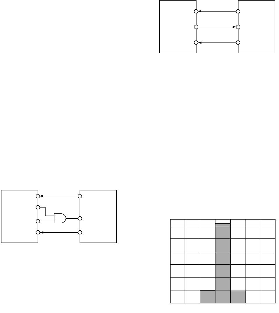
AD7894 to 8X51/L51 Interface
Figure 6 shows an interface between the AD7894 and the
8X51/L51 microcontroller. The 8X51/L51 is configured for its
Mode 0 serial interface mode. The diagram shows the simplest
form of the interface where the AD7894 is the only part con-
nected to the serial port of the 8X51/L51 and, therefore, no
decoding of the serial read operations is required.
To select the AD7894 in systems where more than one device is
connected to the 8X51/L51’s serial port, a port bit, configured
as an output from one of the 8X51/L51’s parallel ports, can be
used to gate on or off the serial clock to the AD7894. A simple
AND function on this port bit and the serial clock from the
8X51/L51 will provide this function. The port bit should be
high to select the AD7894 and low when it is not selected.
The end of conversion can be monitored by using the BUSY
signal, which is shown in the interface diagram of Figure 6.
With the BUSY line from the AD7894 connected to the Port
P1.2 of the 8X51/L51 the BUSY line can be polled by the
8X51/L51. The BUSY line can be connected to the INT1 line
of the 8X51/L51 if an interrupt driven system is preferred.
These two options are shown on the diagram.
Note also that the AD7894 outputs the MSB first during a read
operation while the 8X51/L51 expects the LSB first. Therefore,
the data that is read into the serial buffer needs to be rearranged
before the correct data format from the AD7894 appears in the
accumulator.
The serial clock rate from the 8X51/L51 is limited to signifi-
cantly less than the allowable input serial clock frequency with
which the AD7894 can operate. As a result, the time to read
data from the part will actually be longer than the conversion
time of the part. This means that the AD7894 cannot run at its
maximum throughput rate when used with the 8X51/L51.
P1.2 OR INT1
P3.0
P3.1
SDATA
BUSY
SCLK
AD7894
8X51/L51
Figure 6. AD7894 to 8X51/L51 Interface
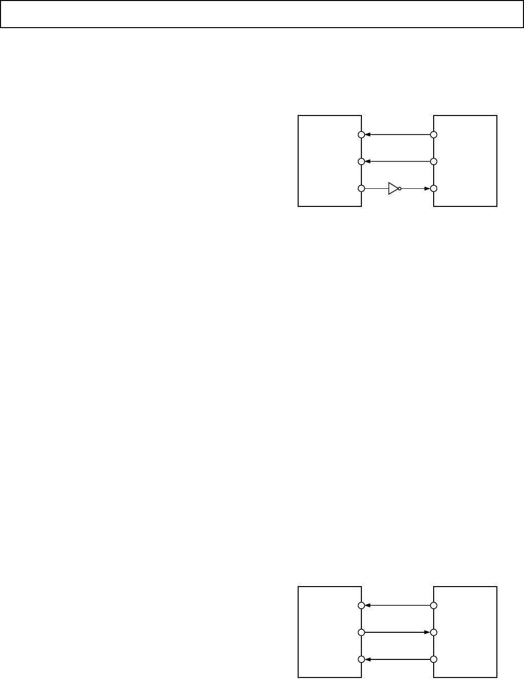
AD7894 to 68HC11/L11 Interface
An interface circuit between the AD7894 and the 68HC11/L11
microcontroller is shown in Figure 7. For the interface shown,
the 68L11 SPI port is used and the 68L11 is configured in its
single-chip mode. The 68L11 is configured in the master mode
with its CPOL bit set to a logic zero and its CPHA bit set to a
logic one. As with the previous interface, the diagram shows the
simplest form of the interface where the AD7894 is the only part
connected to the serial port of the 68L11 and therefore no de-
coding of the serial read operations is required.
Once again, to select the AD7894 in systems where more than
one device is connected to the 68HC11’s serial port, a port bit,
configured as an output from one of the 68HC11’s parallel
ports, can be used to gate on or off the serial clock to the AD7894.
A simple AND function on this port bit and the serial clock
from the 68L11 will provide this function. The port bit should
be high to select the AD7894 and low when it is not selected.
The end of conversion is monitored by using the BUSY signal,
which is shown in the interface diagram of Figure 7. With the
BUSY line from the AD7894 connected to the Port PC2 of the
68HC11/L11 the BUSY line can be polled by the 68HC11/L11.
The BUSY line can be connected to the IRQ line of the 68HC11/
L11 if an interrupt driven system is preferred. These two op-
tions are shown in the diagram.
The serial clock rate from the 68HC11/L11 is limited to signifi-
cantly less than the allowable input serial clock frequency with
which the AD7894 can operate. As a result, the time to read
data from the part will be longer than the conversion time of the
part. This means that the AD7894 cannot run at its maximum
throughput rate when used with the 68HC11/L11.
PC2 OR IRQ
SCK
MISO
SDATA
BUSY
SCLK
AD7894
68HC11/L11
Figure 7. AD7894 to 68HC11/L11 Interface