AD7894
–6–
REV. 0
CONVERTER DETAILS
The AD7894 is a fast, 14-bit single supply A/D converter. It
provides the user with signal scaling, track/hold, A/D converter
and serial interface logic functions on a single chip. The A/D
converter section of the AD7894 consists of a conventional
successive-approximation converter based around an R-2R
ladder structure. The signal scaling on the AD7894-10 and
AD7894-3 allows the part to handle ±10 V and ±2.5 V input
signals respectively while operating from a single +5␣ V supply.
The AD7894-2 accepts an analog input range of 0 V to +2.5 V.
The part requires an external +2.5 V reference. The reference
input to the part is buffered on-chip. The AD7894 has two
operating modes, the high sampling mode and the “auto-sleep”
mode where the part automatically goes into sleep after the end
of conversion. These modes are discussed in more detail in the
Timing and Control Section.
A major advantage of the AD7894 is that it provides all of the
above functions in an 8-lead SOIC package. This offers the user
considerable space saving advantages over alternative solutions.
The AD7894 typically consumes only 20␣ mW, making it ideal
for battery powered applications.
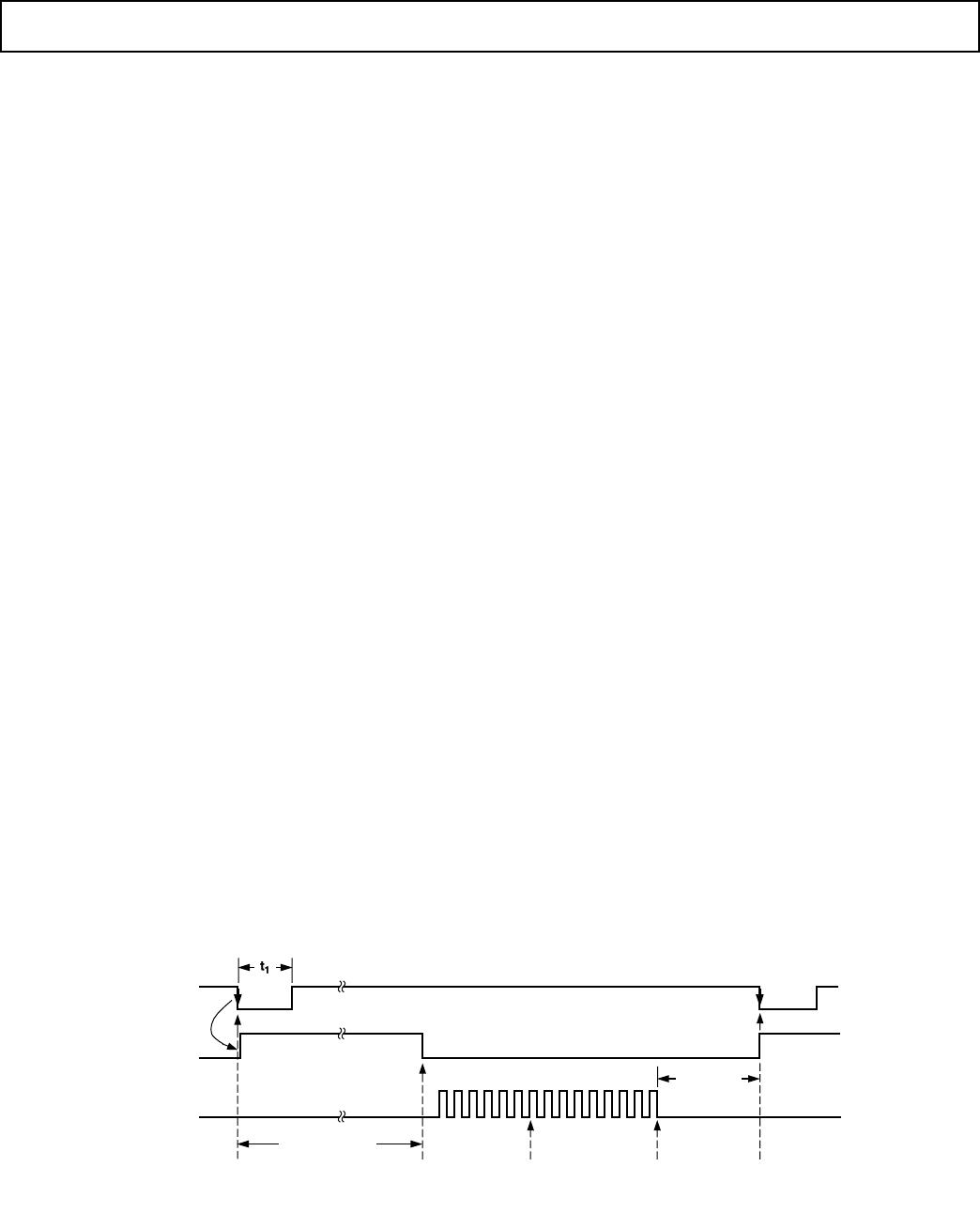
Conversion is initiated on the AD7894 by pulsing the CONVST
input. On the falling edge of CONVST, the on-chip track/hold
goes from track-to-hold mode and the conversion sequence is
started. The conversion clock for the part is generated internally
using a laser-trimmed clock oscillator circuit. Conversion time for
the AD7894 is 5␣ µs in the high sampling mode (10 µs for the auto
sleep mode), and the track/hold acquisition time is 0.35␣ µs. To
obtain optimum performance from the part, the read operation
should not occur during the conversion or during 250 ns prior
to the next conversion. This allows the part to operate at through-
put rates up to 160 kHz and achieve data sheet specifications.
CIRCUIT DESCRIPTION
Analog Input Section
The AD7894 is offered as three part types, the AD7894-10,
which handles a ±10 V input voltage range, the AD7894-3,
which handles input voltage range ±2.5 V and the AD7894-2,
which handles a 0␣ V to +2.5␣ V input voltage range.
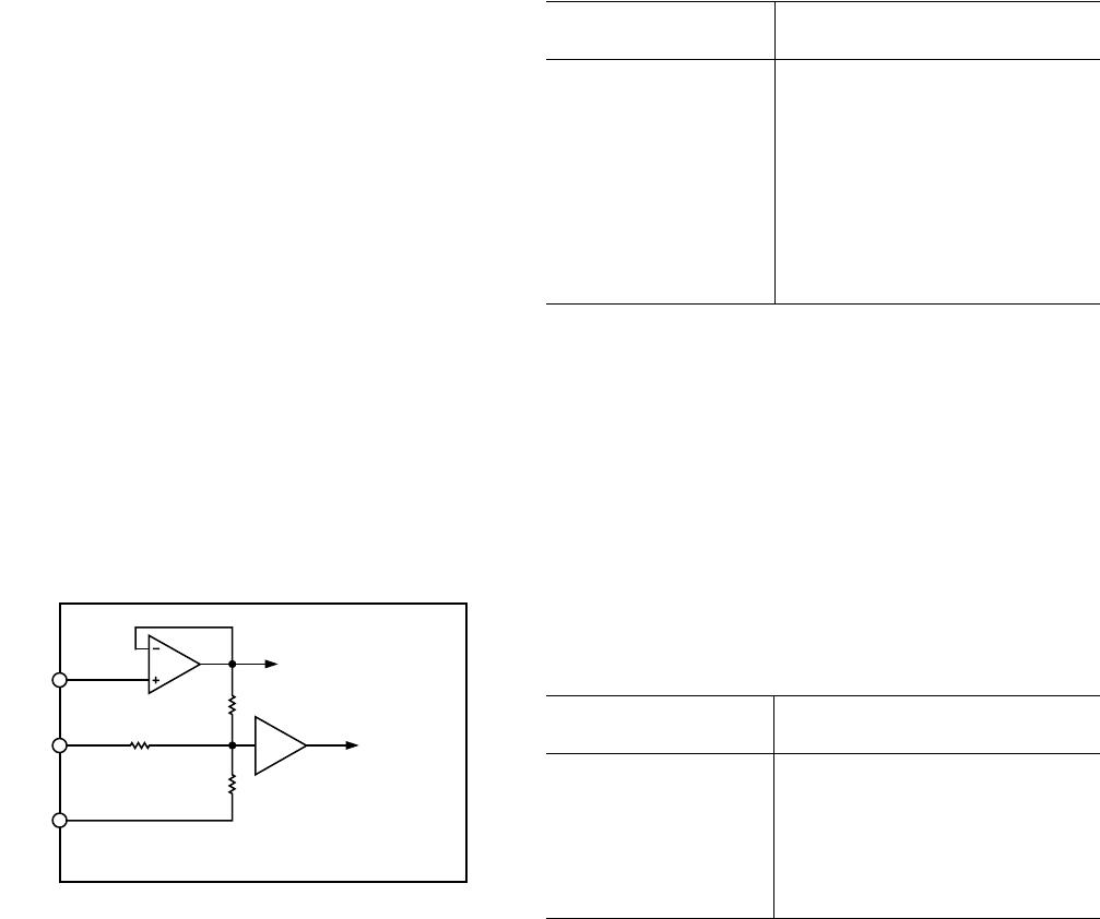
TRACK/
HOLD
AD7894-10/AD7894-3
REF IN
V
IN
GND
R1
R2
R3
TO ADC
REFERENCE
CIRCUITRY
TO INTERNAL
COMPARATOR
Figure 2. AD7894-10/AD7894-3 Analog Input Structure
Figure 2 shows the analog input section for the AD7894-10 and
AD7894-3. The analog input range of the AD7894-10 is ±10 V
and the analog input range for the AD7894-3 is ±2.5 V. This
input is benign, with no dynamic charging currents as the resis-
tor stage is followed by a high input impedance stage of the
track/hold amplifier. For the AD7894-10, R1 = 8 k, R2 = 2 k
and R3 = 2 k. For the AD7894-3, R1 = R2 = 2 k and R3
is open circuit. The current flowing in the analog input is di-
rectly related to the analog input voltage. The maximum input
current flows when the analog input is at negative full scale.
For the AD7894-10 and AD7894-3, the designed code transi-
tions occur on successive integer LSB values (i.e., 1 LSB, 2 LSBs,
3 LSBs . . .). Output coding is twos complement binary with
1 LSB = FS/16384. The ideal input/output transfer function for
the AD7894-10 and AD7894-3 is shown in Table I.
Table I. Ideal Input/Output Code Table for the AD7894-10/
AD7894-3
Digital Output
Analog Input
l
Code Transition
+FSR/2 – 1 LSB
2
011 . . . 110 to 011 . . . 111
+FSR/2 – 2 LSBs 011 . . . 101 to 011 . . . 110
+FSR/2 – 3 LSBs 011 . . . 100 to 011 . . . 101
GND + 1 LSB 000 . . . 000 to 000 . . . 001
GND 111 . . . 111 to 000 . . . 000
GND – 1 LSB 111 . . . 110 to 111 . . . 111
–FSR/2 + 3 LSBs 100 . . . 010 to 100 . . . 011
–FSR/2 + 2 LSBs 100 . . . 001 to 100 . . . 010
–FSR/2 + 1 LSB 100 . . . 000 to 100 . . . 001
NOTES
1
FSR is full-scale range = 20 V (AD7894-10) and = 5 V (AD7894-3) with
REF IN = +2.5 V.
2
1 LSB = FSR/16384 = 1.22 mV (AD7894-10) and 0.3 mV (AD7894-3) with
REF IN = +2.5 V.
The analog input section for the AD7894-2 contains no biasing
resistors and the V
IN
pin drives the input directly to the track/
hold amplifier. The analog input range is 0 V to +2.5 V into a
high impedance stage with an input current of less than 500␣ nA.
This input is benign, with no dynamic charging currents. Once
again, the designed code transitions occur on successive integer
LSB values. Output coding is straight (natural) binary with
1 LSB = FS/16384 = 2.5 V/16384 = 0.15 mV. Table II shows
the ideal input/output transfer function for the AD7894-2.
Table II. Ideal Input/Output Code Table for AD7894-2
Digital Output
Analog Input
1
Code Transition
+FSR – 1 LSB
2
111 . . . 110 to 111 . . . 111
+FSR – 2 LSB 111 . . . 101 to 111 . . . 110
+FSR – 3 LSB 111 . . . 100 to 111 . . . 101
GND + 3 LSB 000 . . . 010 to 000 . . . 011
GND + 2 LSB 000 . . . 001 to 000 . . . 010
GND + 1 LSB 000 . . . 000 to 000 . . . 001
NOTES
1
FSR is full-scale range and is 2.5 V for AD7894-2 with VREF = +2.5 V.
2
1 LSB = FSR/16384 and is 0.15 mV for AD7894-2 with VREF = +2.5 V.
AD7894
–7–REV. 0
Track/Hold Section
The track/hold amplifier on the analog input of the AD7894
allows the ADC to accurately convert an input sine wave of full-
scale amplitude to 14-bit accuracy. The input bandwidth of the
track/hold is greater than the Nyquist rate of the ADC, even
when the ADC is operated at its maximum throughput rate of
160 kHz (i.e., the track/hold can handle input frequencies in
excess of 100 kHz).
The track/hold amplifier acquires an input signal to 14-bit accu-
racy in less than 0.35␣ µs. The operation of the track/hold is
essentially transparent to the user. With the high sampling
operating mode the track/hold amplifier goes from its tracking
mode to its hold mode at the start of conversion (i.e., the falling
edge of CONVST). The aperture time for the track/hold (i.e.,
the delay time between the external CONVST signal and the
track/hold actually going into hold) is typically 15␣ ns. At the
end of conversion (on the falling edge of BUSY) the part re-
turns to its tracking mode. The acquisition time of the track/
hold amplifier begins at this point. For the auto shutdown mode,
the rising edge of CONVST wakes up the part and the track
and hold amplifier goes from its tracking mode to its hold mode
5 µs after the rising edge of CONVST (provided that the
CONVST high time is less than 5 µs). Once again the part re-
turns to its tracking mode at the end of conversion when the
BUSY signal goes low.
Reference Input
The reference input to the AD7894 is buffered on-chip with a
maximum reference input current of 1␣ µA. The part is specified
with a +2.5 V reference input voltage. Errors in the reference
source will result in gain errors in the AD7894’s transfer func-
tion and will add to the specified full-scale errors on the part.
Suitable reference sources for the AD7894 include the AD780
and AD680 precision +2.5 V references.
Timing and Control Section
Figure 3 shows the timing and control sequence required to
obtain optimum performance from the AD7894. In the se-
quence shown, conversion is initiated on the falling edge of
CONVST and new data from this conversion is available in the
output register of the AD7894 5␣ µs later. Once the read opera-
tion has taken place, a further 250␣ ns should be allowed before
the next falling edge of CONVST to optimize the settling of the
track/hold amplifier before the next conversion is initiated.
With the serial clock frequency at its maximum of 16␣ MHz, the
achievable throughput rate for the part is 5␣ µs (conversion
time) plus 1.0␣ µs (read time) plus 250␣ ns (quiet time). This
results in a minimum throughput time of 6.25␣ µs (equivalent to
a throughput rate of 160 kHz). A serial clock of less than 16 MHz
can be used, but this will in turn mean that the throughput
time will increase.
The read operation consists of 16 serial clock pulses to the
output shift register of the AD7894. After 16 serial clock pulses
the shift register is reset and the SDATA line is three-stated. If
there are more serial clock pulses after the 16th clock, the shift
register will be moved on past its reset state. However, the shift
register will be reset again on the falling edge of the CONVST
signal to ensure that the part returns to a known state every
conversion cycle. As a result, a read operation from the output
register should not straddle across the falling edge of CONVST
as the output shift register will be reset in the middle of the
read operation and the data read back into the microprocessor
will appear invalid.
OPERATING MODES
Mode 1 Operation (High Sampling Performance)
The timing diagram in Figure 3 is for optimum performance in
operating Mode 1 where the falling edge of CONVST starts
conversion and puts the Track/Hold amplifier into its hold
mode. This falling edge of CONVST also causes the BUSY
signal to go high to indicate that a conversion is taking place.
The BUSY signal goes low when the conversion is complete,
which is 5 µs max after the falling edge of CONVST and new
data from this conversion is available in the output register of
the AD7894. A read operation accesses this data. This read
operation consists of 16 clock cycles and the length of this read
operation will depend on the serial clock frequency. For the
fastest throughput rate (with a serial clock of 16 MHz) the read
operation will take 1.0 µs. The read operation must be com-
plete at least 250 ns before the falling edge of the next CONVST
and this gives a total time of 6.25 µs for the full throughput
time (equivalent to 160 kHz). This mode of operation should
be used for high sampling applications.
250ns MIN
t
1
= 40ns MIN
t
CONVERT
= 5ms
BUSY
SCLK
CONVST
CONVERSION IS
INITIATED;
TRACK/HOLD
GOES INTO HOLD
CONVERSION
ENDS
5ms LATER
SERIAL READ
OPERATION
READ OPERATION
SHOULD END
250ns PRIOR TO
NEXT FALLING
EDGE OF CONVST
OUTPUT
SERIAL
SHIFT
REGISTER
IS RESET
Figure 3. Mode 1 Timing Operation Diagram for High Sampling Performance
AD7894
–8–
REV. 0
250ns MIN
BUSY
SCLK
CONVST
CONVERSION
IS INITIATED;
TRACK/HOLD
GOES INTO
HOLD
CONVERSION
ENDS
10ms LATER
SERIAL READ
OPERATION
READ OPERATION
SHOULD END 250ns
PRIOR TO NEXT
RISING EDGE OF
CONVST
OUTPUT
SERIAL SHIFT
REGISTER
IS RESET
t
CONVERT
= 10ms
PART
WAKES
UP
Figure 4. Mode 2 Timing Diagram Where Automatic Sleep Function is Initiated
t
2
t
3
t
4
t
5
t
6
2 LEADING
ZEROS
THREE-STATE
THREE-
STATE
1 2 3 4 15 16
DB13 DB12 DB0
SCLK (I/P)
DOUT (O/P)
t
2
= t
3
= 31.25ns MIN, t
4
= 60ns MAX, t
5
= 10ns MIN, t
6
= 20ns MAX @ 5V, A, B, VERSIONS
Figure 5. Data Read Operation
Mode 2 Operation (Auto Sleep After Conversion)
The timing diagram in Figure 4 is for optimum performance in
operating Mode 2, where the part automatically goes into sleep
mode once BUSY goes low, after conversion and “wakes up”
before the next conversion takes place. This is achieved by keep-
ing CONVST low at the end of conversion, whereas it was high
at the end of conversion for Mode 1 Operation. The rising edge
of CONVST “wakes up” the AD7894. This wake-up time is
typically 5 µs and is controlled internally by a monostable cir-
cuit. While the AD7894 is waking up there is some digital activ-
ity internal to the part. If the falling edge of CONVST (putting
the track/hold amplifier into hold mode) should occur during
this digital activity, noise will be injected into the track/hold
amplifier resulting in a poor conversion. For optimum results
the CONVST pulse should be between 40 ns and 2 µs or greater
than 6 µs in width. The narrower pulse will allow a system to
instruct the AD7894 to begin waking up and perform a conver-
sion when ready, whereas the pulse greater than 6 µs will give
control over when the sampling instant takes place. Note that
the 10 µs wake-up time shown in Figure 4 is for a CONVST pulse
less than 2 µs. If a CONVST pulse greater than 6 µs is used, the
conversion will not complete for a further 5 µs after the falling edge
of CONVST. Even though the part is in sleep mode, data can still
be read from it. The read operation consists of 16 clock cycles as in
Mode 1 Operation. For the fastest serial clock of 16 MHz, the read
operation will take 1.0 µs and this must be complete at least 250 ns
before the falling edge of the next CONVST, to allow the track/
hold amplifier to have enough time to settle. This mode is very
useful when the part is converting at a slow rate, as the power
consumption will be significantly reduced from that of Mode 1
Operation.
Serial Interface
The serial interface to the AD7894 consists of just three wires, a
serial clock input (SCLK) and the serial data output (SDATA)
and a conversion status output (BUSY). This allows for an
easy-to-use interface to most microcontrollers, DSP processors
and shift registers.
Figure 5 shows the timing diagram for the read operation to the
AD7894. The serial clock input (SCLK) provides the clock
source for the serial interface. Serial data is clocked out from
the SDATA line on the falling edge of this clock and is valid on
both the rising and falling edges of SCLK. The advantage of
having the data valid on both the rising and falling edges of the
SCLK is to give the user greater flexibility in interfacing to the
part and so a wider range of microprocessor and microcontrol-
ler interfaces can be accommodated. This also explains the two
timing figures, t
4
and t
5
, that are quoted on the diagram. The
time t
4
specifies how long after the falling edge of the SCLK the
next data bit becomes valid, whereas the time t
5
specifies for
how long after the falling edge of the SCLK the current data bit
is valid. The first leading zero is clocked out on the first rising
edge of SCLK. Note that the first zero will be valid on the first
falling edge of SCLK even though the data access time is speci-
fied at 60 ns for the other bits. The reason for this is that the
first bit will be clocked out faster than the other bits is due to
the internal architecture of the part. Sixteen clock pulses must
be provided to the part to access to full conversion result. The
AD7894 provides two leading zeros followed by the 14-bit
conversion result starting with the MSB (DB13). The last data
bit to be clocked out on the penultimate falling clock edge is the
LSB (DB0). On the 16th falling edge of SCLK the LSB (DB0)
will be valid for a specified time to allow the bit to be read on
the falling edge of the SCLK and then the SDATA line is dis-
abled (three-stated). After this last bit has been clocked out,
the SCLK input should return low and remain low until the
next serial data read operation. If there are extra clock pulses
after the 16th clock, the AD7894 will start over again with
outputting data from its output register and the data bus will
no longer be three-stated even when the clock stops. Provided
the serial clock has stopped before the next falling edge of

AD7894BRZ-10

Mfr. #:
Manufacturer:
Analog Devices Inc.
Description:
Analog to Digital Converters - ADC Bipolar Input 5V 14B Serial 4.5uS
Lifecycle:
New from this manufacturer.
Delivery:
DHL FedEx Ups TNT EMS
Payment:
T/T Paypal Visa MoneyGram Western Union