General Description
The MAX5054–MAX5057 dual, high-speed MOSFET
drivers source and sink up to 4A peak current. These
devices feature a fast 20ns propagation delay and 20ns
rise and fall times while driving a 5000pF capacitive
load. Propagation delay time is minimized and matched
between the inverting and noninverting inputs and
between channels. High sourcing/sinking peak cur-
rents, low propagation delay, and thermally enhanced
packages make the MAX5054–MAX5057 ideal for high-
frequency and high-power circuits.
The MAX5054–MAX5057 operate from a 4V to 15V single
power supply and consume 40µA (typ) of supply current
when not switching. These devices have internal logic
circuitry that prevents shoot-through during output state
changes to minimize the operating current at high
switching frequency. The logic inputs are protected
against voltage spikes up to +18V, regardless of the V
DD
voltage. The MAX5054A is the only version that has
CMOS input logic levels while the MAX5054B/MAX5055/
MAX5056/MAX5057 have TTL input logic levels.
The MAX5055–MAX5057 provide the combination of dual
inverting, dual noninverting, and inverting/noninverting
input drivers. The MAX5054 feature both inverting and
noninverting inputs per driver for greater flexibility. They
are available in 8-pin TDFN (3mm x 3mm), standard SO,
and thermally enhanced SO packages. These devices
operate over the automotive temperature range of -40°C
to +125°C.
Applications
Power MOSFET Switching Motor Control
Switch-Mode Power Supplies Power-Supply Modules
DC-DC Converters
Features
o 4V to 15V Single Power Supply
o 4A Peak Source/Sink Drive Current
o 20ns (typ) Propagation Delay
o Matching Delay Between Inverting and
Noninverting Inputs
o Matching Propagation Delay Between Two
Channels
o V
DD
/ 2 CMOS Logic Inputs (MAX5054AATA)
o TTL Logic Inputs
(MAX5054B/MAX5055/MAX5056/MAX5057)
o 0.1 x V
DD
(CMOS) and 0.3V (TTL) Logic-Input
Hysteresis
o Up to +18V Logic Inputs (Regardless of V
DD
Voltage)
o Low Input Capacitance: 2.5pF (typ)
o 40µA (typ) Quiescent Current
o -40°C to +125°C Operating Temperature Range
o 8-Pin TDFN and SO Packages
MAX5054–MAX5057
4A, 20ns, Dual MOSFET Drivers
________________________________________________________________
Maxim Integrated Products
1
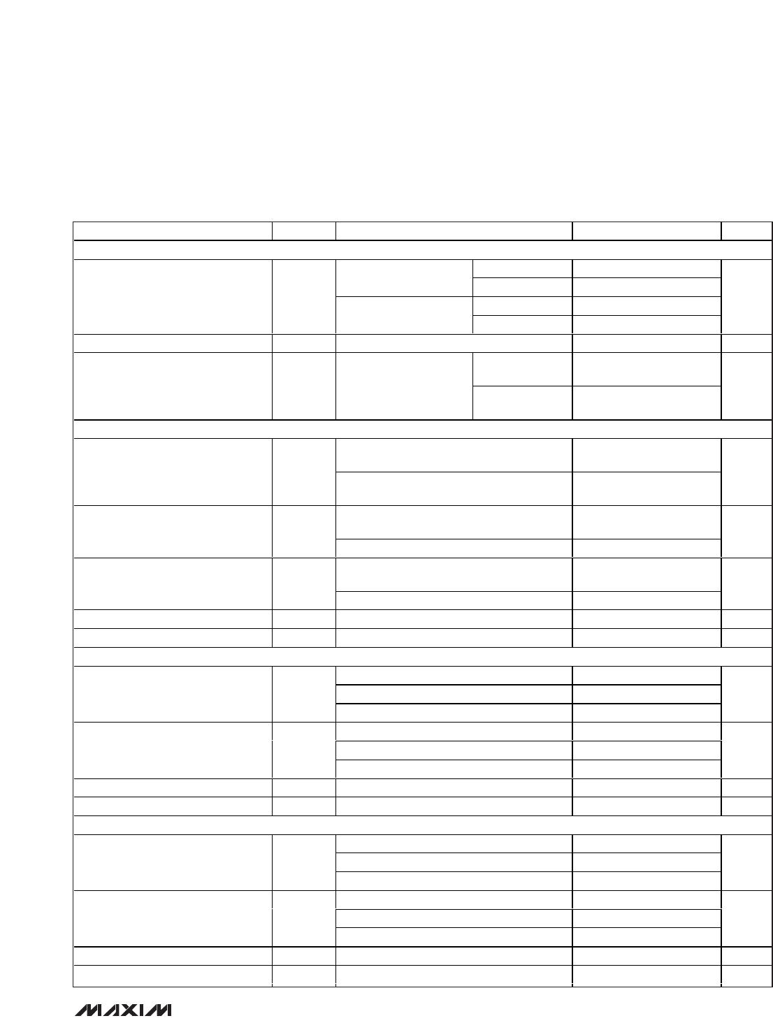
Ordering Information
MAX5054
INA+
INA-
INB+
INB-
OUTB
OUTA
V
DD
GND
PWM IN
V
OUT
V
IN
Typical Operating Circuit
19-3348; Rev 3; 3/11
For pricing, delivery, and ordering information, please contact Maxim/Dallas Direct! at
1-888-629-4642, or visit Maxim’s website at www.maxim-ic.com.
*
EP = Exposed pad.
/V
Denotes an automotive qualified part.
+
Denotes a lead(Pb)-free/RoHS-compliant package.
PART
TEMP
RANGE
PIN-
PACKAGE
TOP
MARK
MAX5054AATA+ -40°C to +125°C 8 TDFN-EP* AGS
MAX5054AATA/V+ -40°C to +125°C 8 TDFN-EP* BMF
MAX5054BATA+ -40°C to +125°C 8 TDFN-EP* AGR
MAX5055AASA+ -40°C to +125°C 8 SO-EP*
MAX5055BASA+ -40°C to +125°C 8 SO
MAX5056AASA+ -40°C to +125°C 8 SO-EP*
MAX5056BASA+ -40°C to +125°C 8 SO
MAX5057AASA+ -40°C to +125°C 8 SO-EP*
MAX5057BASA+ -40°C to +125°C 8 SO
Selector Guide and Pin Configurations appear at end of
data sheet.
4A, 20ns, Dual MOSFET Drivers
2 _______________________________________________________________________________________
ABSOLUTE MAXIMUM RATINGS
ELECTRICAL CHARACTERISTICS
(V
DD
= 4V to 15V, T
A
= -40°C to +125°C, unless otherwise noted. Typical values are at V
DD
= 15V and T
A
= +25°C.) (Note 2)
Stresses beyond those listed under “Absolute Maximum Ratings” may cause permanent damage to the device. These are stress ratings only, and functional
operation of the device at these or any other conditions beyond those indicated in the operational sections of the specifications is not implied. Exposure to
absolute maximum rating conditions for extended periods may affect device reliability.
(Voltages referenced to GND.)
V
DD
...............................................................................-0.3V to +18V
INA+, INA-, INB+, INB- ...............................................-0.3V to +18V
OUTA, OUTB...................................................-0.3V to (V
DD
+ 0.3V)
OUTA, OUTB Short-Circuit Duration ........................................10ms
Continuous Source/Sink Current at OUT_ (P
D
< P
DMAX
) .....200mA
Continuous Power Dissipation (T
A
= +70°C)
8-Pin TDFN-EP (derate 18.2mW/°C above +70°C)........1454mW
8-Pin SO-EP (derate 19.2mW/°C above +70°C)… ........1538mW
8-Pin SO (derate 5.9mW/°C above +70°C)… ..................471mW
Operating Temperature Range..............................-40°C to +125°C
Storage Temperature Range .................................-65°C to +150°C
Junction Temperature ...........................................................+150°C
Lead Temperature (soldering, 10s)......................................+300°C
Soldering Temperature (reflow)............................................+260°C
PACKAGE THERMAL CHARACTERISTICS (Note 1)
MAX5054–MAX5057
PARAMETER SYMBOL CONDITIONS MIN TYP MAX UNITS
POWER SUPPLY
V
DD
Operating Range V
DD
415V
V
DD
Undervoltage Lockout UVLO V
DD
rising 3.00 3.50 3.85 V
V
DD
Undervoltage Lockout
Hysteresis
200 mV
V
DD
Undervoltage Lockout to
Output Delay
V
DD
rising 12 µs
V
DD
= 4V 28 55
I
DD
INA- = INB- = V
DD
,
INA+ = INB+ = 0V
(not switching)
V
DD
= 15V 40 75
µA
V
DD
Supply Current
I
DD-SW
INA- = 0V, INB+ = V
DD
= 15V,
INA+ = INB- both channels switching at
250kHz, C
L
= 0F
1 2.4 4 mA
DRIVER OUTPUT (SINK)
T
A
= +25°C 1.1 1.8
V
DD
= 15V,
I
OUT_
= -100mA
T
A
= +125°C 1.5 2.4
T
A
= +25°C 2.2 3.3
Driver Output Resistance Pulling
Down
R
ON-N
V
DD
= 4.5V,
I
OUT_
= -100mA
T
A
= +125°C 3.0 4.5
Peak Output Current (Sinking) I
PK-N
V
DD
= 15V, C
L
= 10,000pF 4 A
V
DD
= 4.5V 0.45
Output-Voltage Low I
OUT_
= -100mA
V
DD
= 15V 0.24
V
Latchup Protection I
LUP
Reverse current I
OUT_
(Note 2) 400 mA
8 TDFN-EP
Junction-to-Ambient Thermal Resistance (θ
JA
)...............+41°C/W
Junction-to-Case Thermal Resistance (θ
JC
)......................+8°C/W
8 SO
Junction-to-Ambient Thermal Resistance (θ
JA
)................+132°C/W
Junction-to-Case Thermal Resistance (θ
JC
).......................+40°C/W
8 SO-EP
Junction-to-Ambient Thermal Resistance (θ
JA
)..................+41°C/W
Junction-to-Case Thermal Resistance (θ
JC
)......................+7°C/W
Note 1: Package thermal resistances were obtained using the method described in JEDEC specification JESD51-7, using a four-
layer board. For detailed information on package thermal considerations, refer to www.maxim-ic.com/thermal-tutorial
.
MAX5054–MAX5057
4A, 20ns, Dual MOSFET Drivers
_______________________________________________________________________________________ 3
ELECTRICAL CHARACTERISTICS (continued)
(V
DD
= 4V to 15V, T
A
= -40°C to +125°C, unless otherwise noted. Typical values are at V
DD
= 15V and T
A
= +25°C.) (Note 2)
PARAMETER SYMBOL CONDITIONS MIN TYP MAX UNITS
DRIVER OUTPUT (SOURCE)
T
A
= +25°C 1.5 2.1
V
DD
= 15V,
I
OUT_
= 100mA
T
A
= +125°C 1.9 2.75
T
A
= +25°C 2.75 4
Driver Output Resistance Pulling
Up
R
ON-P
V
DD
= 4.5V,
I
OUT_
= 100mA
T
A
= +125°C 3.75 5.5
Peak Output Current (Sourcing) I
PK-P
V
DD
= 15V, C
L
= 10,000pF 4 A
V
DD
= 4.5V
V
DD
-
0.55
Output-Voltage High I
OUT_
= 100mA
V
DD
= 15V
V
DD
-
0.275
V
LOGIC INPUT (Note 4)
MAX5054A
0.7 x
V
DD
Logic 1 Input Voltage V
IH
MAX5054B/MAX5055/MAX5056/MAX5057
(Note 5)
2.1
V
MAX5054A
0.3 x
V
DDLogic 0 Input Voltage V
IL
MAX5054B/MAX5055/MAX5056/MAX5057 0.8
V
MAX5054A
0.1 x
V
DDLogic-Input Hysteresis V
HYS
MAX5054B/MAX5055/MAX5056/MAX5057 0.3
V
Logic-Input-Current Leakage INA+, INB+, INA-, INB- = 0V or V
DD
-1 +0.1 +1 µA
Input Capacitance C
IN
2.5 pF
SWITCHING CHARACTERISTICS FOR V
DD
= 15V (Figure 1)
C
L
= 1000pF 4
C
L
= 5000pF 18
OUT_ Rise Time t
R
C
L
= 10,000pF 32
ns
C
L
= 1000pF 4
C
L
= 5000pF 15OUT_ Fall Time t
F
C
L
= 10,000pF 26
ns
Turn-On Delay Time t
D-ON
C
L
= 10,000pF (Note 3) 10 20 34 ns
Turn-Off Delay Time t
D-OFF
C
L
= 10,000pF (Note 3) 10 20 34 ns
SWITCHING CHARACTERISTICS FOR V
DD
= 4.5V (Figure 1)
C
L
= 1000pF 7
C
L
= 5000pF 37
OUT_ Rise Time t
R
C
L
= 10,000pF 85
ns
C
L
= 1000pF 7
C
L
= 5000pF 30OUT_ Fall Time t
F
C
L
= 10,000pF 75
ns
Turn-On Delay Time t
D-ON
C
L
= 10,000pF (Note 3) 18 35 70 ns
Turn-Off Delay Time t
D-OFF
C
L
= 10,000pF (Note 3) 18 35 70 ns

MAX5055AASA+T

Mfr. #:
Manufacturer:
Maxim Integrated
Description:
Gate Drivers 4A 20ns Dual MOSFET Drivers
Lifecycle:
New from this manufacturer.
Delivery:
DHL FedEx Ups TNT EMS
Payment:
T/T Paypal Visa MoneyGram Western Union