General Description
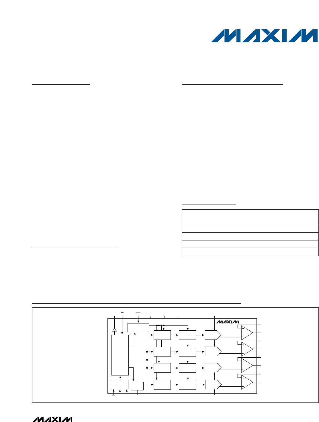
The MAX5500/MAX5501 integrate four low-power, 12-bit
digital-to analog converters (DACs) and four precision
output amplifiers in a small, 20-pin package. Each nega-
tive input of the four precision amplifiers is externally
accessible providing flexibility in gain configurations,
remote sensing, and high output drive capacity, making
the MAX5500/MAX5501 ideal for industrial-process-con-
trol applications. Other features include software shut-
down, hardware shutdown lockout, an active-low reset
which clears all registers and DACs to zero, a user-pro-
grammable logic output, and a serial-data output.
Each DAC provides a double-buffered input organized
as an input register followed by a DAC register. A 16-bit
serial word loads data into each input register. The seri-
al interface is compatible with SPI™/QSPI™/
MICROWIRE™. The serial interface allows the input and
DAC registers to be updated independently or simulta-
neously with a single software command. The 3-wire
interface simultaneously updates the DAC registers. All
logic inputs are TTL/CMOS-logic compatible. The
MAX5500 operates from a single +5V power supply,
and the MAX5501 operates from a single +3V power
supply. The MAX5500/MAX5501 are specified over the
extended -40°C to +105°C temperature range.
Applications
Industrial Process Controls
Automatic Test Equipment
Microprocessor (μP)-Controlled Systems
Motion Control
Digital Offset and Gain Adjustment
Remote Industrial Controls
Features
o Four 12-Bit DACs with Configurable Output
Amplifiers
o +5V or +3V Single-Supply Operation
o Low Supply Current:
0.85mA Normal Operation
10µA Shutdown Mode (MAX5500)
o Force-Sense Outputs
o Power-On Reset Clears All Registers and DACs
to Zero
o Capable of Recalling Last State Prior to Shutdown
o SPI/QSPI/MICROWIRE Compatible
o Simultaneous or Independent Control of DACs
through 3-Wire Serial Interface
o User-Programmable Digital Output
o Guaranteed Over Extended Temperature Range
(-40°C to +105°C)
MAX5500/MAX5501
Low-Power, Quad, 12-Bit
Voltage-Output DACs with Serial Interface
________________________________________________________________
Maxim Integrated Products
1
MAX5500
MAX5501
OUTA
FBA
FBB
FBC
FBD
DAC A
DAC B
DAC C
DAC D
REFAB
DAC
REGISTER A
DECODE
CONTROL
INPUT
REGISTER A
DAC
REGISTER B
INPUT
REGISTER B
DAC
REGISTER C
INPUT
REGISTER C
DAC
REGISTER D
INPUT
REGISTER D
16-BIT
SHIFT
REGISTER
SR
CONTROL
LOGIC
OUTPUT
CS
DIN
SCLK
OUTB
OUTC
OUTD
DOUT
PDL
CL
V
DD
AGND
DGND
UPO REFCD
Functional Diagram
19-4368; Rev 1; 4/09
For pricing, delivery, and ordering information, please contact Maxim Direct at 1-888-629-4642,
or visit Maxim’s website at www.maxim-ic.com.
Pin Configuration appears at end of data sheet.
SPI/QSPI are trademarks of Motorola, Inc. MICROWIRE is a trademark of National Semiconductor, Corp.
Ordering Information
PART
PIN-
PACKAGE
INL (LSB)
SUPPLY (V)
MAX5500AGAP+ 20 SSOP ±0.75 +5
MAX5500BGAP+ 20 SSOP ±2 +5
MAX5501AGAP+ 20 SSOP ±0.75 +3
MAX5501BGAP+ 20 SSOP ± 2 +3
+
Denotes a lead(Pb)-free/RoHS-compliant package.
Note: All devices are specified over the -40°C to +105°C operating
temperature range.
MAX5500/MAX5501
Low-Power, Quad, 12-Bit
Voltage-Output DACs with Serial Interface
2 _______________________________________________________________________________________
ABSOLUTE MAXIMUM RATINGS
ELECTRICAL CHARACTERISTICS
(MAX5500 (V
DD
= +5V ±10%, V
REFAB
= V
REFCD
= 2.5V), MAX5501 (V
DD
= +3V to +3.6V, V
REFAB
= V
REFCD
= 1.25V), V
AGND
= V
DGND
= 0, R
L
= 5k, C
L
= 100pF, T
A
= T
MIN
to T
MAX
, unless otherwise noted. Typical values at T
A
= +25°C. Output buffer connected in
unity-gain configuration (Figure 9).)
Stresses beyond those listed under “Absolute Maximum Ratings” may cause permanent damage to the device. These are stress ratings only, and functional
operation of the device at these or any other conditions beyond those indicated in the operational sections of the specifications is not implied. Exposure to
absolute maximum rating conditions for extended periods may affect device reliability.
V
DD
to AGND............................................................-0.3V to +6V
V
DD
to DGND ...........................................................-0.3V to +6V
AGND to DGND.....................................................-0.3V to +0.3V
REFAB, REFCD to AGND...........................-0.3V to (V
DD
+ 0.3V)
OUT_, FB_ to AGND...................................-0.3V to (V
DD
+ 0.3V)
Digital Inputs to DGND.............................................-0.3V to +6V
DOUT, UPO to DGND ................................-0.3V to (V
DD
+ 0.3V)
Continuous Current into Any Pin.......................................±20mA
Continuous Power Dissipation (T
A
= +70°C)
20-Pin SSOP (derate 8.00mW/°C above +70°C) .........640mW
Operating Temperature Range .........................-40°C to +105°C
Storage Temperature Range .............................-65°C to +150°C
Lead Temperature (soldering, 10s) .................................+300°C
PARAMETER SYMBOL CONDITIONS MIN TYP MAX UNITS
STATIC PERFORMANCE (Analog Section)
Resolution N 12 Bits
MAX5500A/MAX5501A ±0.25 ±0.75
Integral Nonlinearity
(Note 1)
INL
MAX5500B/MAX5501B ±2.0
LSB
Differential Nonlinearity DNL Guaranteed monotonic ±1.0 LSB
Offset Error V
OS
±3.5 mV
Offset-Error Tempco 6 ppm/
o
C
MAX5500 -0.3 ±2.0
Gain Error (Note 1) GE
MAX5501 -0.7 ±4.0
LSB
Gain-Error Tempco 1 ppm/
o
C
MAX5500 100 600
Power-Supply Rejection Ratio PSRR
MAX5501 100 300
µV/V
MATCHING PERFORMANCE (T
A
= +25
o
C)
MAX5500 -0.3 ±2.0
Gain Error GE
MAX5501 -0.85 ±4.0
LSB
Offset Error V
OS
±1.0 ±3.5 mV
Integral Nonlinearity INL (Note 1) ±0.35 ±1.0 LSB
REFERENCE INPUT
Reference Input Range V
REF
0V
DD
- 1.4 V
Reference Input Resistance R
REF
Code-dependent, minimum at code
555H
8k
Refer ence C ur r ent i n S hutd ow n 0.01 ±1.0 µA
DIGITAL INPUTS
MAX5500A/MAX5500B 2.4
Input High Voltage V
IH
MAX5501A/MAX5501B 2.0
V
Input Low Voltage V
IL
0.8 V
Input Leakage Current I
IN
V
IN
= 0 or V
DD
±0.1 ±1.0 µA
Input Capacitance C
IN
8pF
MAX5500/MAX5501
Low-Power, Quad, 12-Bit
Voltage-Output DACs with Serial Interface
_______________________________________________________________________________________ 3
ELECTRICAL CHARACTERISTICS (continued)
(MAX5500 (V
DD
= +5V ±10%, V
REFAB
= V
REFCD
= 2.5V), MAX5501 (V
DD
= +3V to +3.6V, V
REFAB
= V
REFCD
= 1.25V), V
AGND
= V
DGND
= 0, R
L
= 5k, C
L
= 100pF, T
A
= T
MIN
to T
MAX
, unless otherwise noted. Typical values at T
A
= +25°C. Output buffer connected in
unity-gain configuration (Figure 9).)
PARAMETER SYMBOL CONDITIONS MIN TYP MAX UNITS
DIGITAL OUTPUTS
Output High Voltage V
OH
I
SOURCE
= 2mA V
DD
- 0.5 V
Output Low Voltage V
OL
I
SINK
= 2mA 0.13 0.4 V
DYNAMIC PERFORMANCE
Voltage Output Slew Rate SR 0.6 V/µs
To ±0.5 LSB, V
STEP
= 2.5V
MAX5500A/MAX5500B
12
Output Settling Time
To ±0.5 LSB, V
STEP
= 1.25V
MAX5501A/MAX5501B
16
µs
Output Voltage Swing Rail-to-rail (Note 2) 0 to V
DD
V
Current into FB_ 0 0.1 µA
OUT_ Leakage Current in
Shutdown
R
L
= ±0.01 ±1.0 µA
MAX5500A/MAX5500B 15
Startup Time Exiting
Shutdown Mode
MAX5501A/MAX5501B 20
µs
Digital Feedthrough CS
=V
DD
, f
IN
= 100kHz 5 nVs
Digital Crosstalk 5nVs
POWER SUPPLIES
MAX5500A/MAX5500B 4.5 5.5
Supply Voltage V
DD
MAX5501A/MAX5501B 3.0 3.6
V
Supply Current I
DD
(Note 3) 0.85 1.1 mA
Supply Current in Shutdown (Note 3) 10 20 µA
TIMING CHARACTERISTICS (Figure 6)
SCLK Clock Period t
CP
100 ns
SCLK Pulse-Width High t
CH
40 ns
SCLK Pulse-Width Low t
CL
40 ns
CS Fall to SCLK Rise Setup
Time
t
CSS
40 ns
SCLK Rise to CS Rise Hold
Time
t
CSH
0ns
DIN Setup Time t
DS
40 ns
DIN Hold Time t
DH
0ns

MAX5500AGAP+

Mfr. #:
Manufacturer:
Maxim Integrated
Description:
Digital to Analog Converters - DAC 12-Bit 4Ch Precision DAC
Lifecycle:
New from this manufacturer.
Delivery:
DHL FedEx Ups TNT EMS
Payment:
T/T Paypal Visa MoneyGram Western Union