MAX5500/MAX5501
Low-Power, Quad, 12-Bit
Voltage-Output DACs with Serial Interface
______________________________________________________________________________________ 13
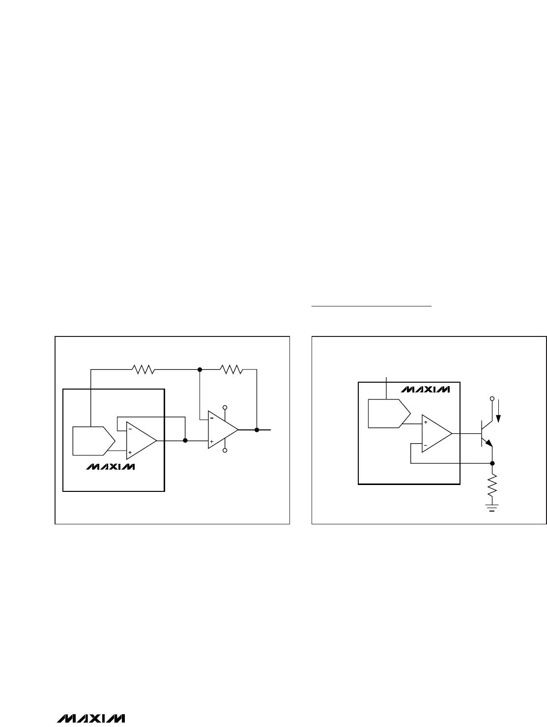
Digitally Programmable Current Source
The circuit of Figure 12 places an npn transistor
(2N3904 or similar) within the op-amp feedback loop to
implement a digitally programmable, unidirectional cur-
rent source. This circuit drives 4mA to 20mA current
loops, which are commonly used in industrial-control
applications. The output current is calculated with the
following equation:
I
OUT
= (V
REF
/R) x (NB/4096)
where NB is the numeric value of the DAC’s binary input
code and R is the sense resistor shown in Figure 12.
Power-Supply Considerations
On power-up, all input and DAC registers are cleared
(set to zero code) and D
OUT
is in mode 0 (serial data is
shifted out of DOUT on the clock’s falling edge).
For rated MAX5500/MAX5501 performance, limit V
REFAB
/
V
REFCD
to 1.4V below V
DD
. Bypass V
DD
with a 4.7µF
capacitor in parallel with a 0.1µF capacitor to AGND.
Use short lead lengths and place the bypass capaci-
tors as close as possible to the supply inputs.
Grounding and Layout Considerations
Digital or AC transient signals between AGND and
DGND create noise at the analog outputs. Connect
AGND and DGND together at the DAC, and then con-
nect this point to the highest-quality ground available.
Good PCB ground layout minimizes crosstalk between
DAC outputs, reference inputs, and digital inputs.
Reduce crosstalk by keeping analog lines away from
digital lines. Do not use wire-wrapped boards.
Chip Information
PROCESS: BiCMOS
DAC
V
OUT
+5V
-5V
R1 = R2 = 10k ± 0.1%
MAX5500
MAX5501
REF_
R1
R2
FB_
OUT_
Figure 11. Bipolar Output Circuit
DAC_
MAX5500
MAX5501
REF_
OUT_
R
I
OUT
2N3904
V
L
FB_
Figure 12. Digitally Progammable Current Source
MAX5500/MAX5501
Low-Power, Quad, 12-Bit
Voltage-Output DACs with Serial Interface
14 ______________________________________________________________________________________
Package Information
For the latest package outline information and land patterns, go
to www.maxim-ic.com/packages
.
PACKAGE TYPE PACKAGE CODE DOCUMENT NO.
20 SSOP A20-2
21-0056
20
19
18
17
16
15
14
13
1
2
3
4
5
6
7
8
V
DD
FBD
OUTD
OUTCOUTB
OUTA
FBA
AGND
TOP VIEW
FBC
REFCD
PDL
UPOCS
CL
REFAB
FBB
12
11
9
10
DOUT
DGNDSCLK
DIN
SSOP
MAX5500
MAX5501
+
Pin Configuration
MAX5500/MAX5501
Low-Power, Quad, 12-Bit
Voltage-Output DACs with Serial Interface
Maxim cannot assume responsibility for use of any circuitry other than circuitry entirely embodied in a Maxim product. No circuit patent licenses are
implied. Maxim reserves the right to change the circuitry and specifications without notice at any time.
Maxim Integrated Products, 120 San Gabriel Drive, Sunnyvale, CA 94086 408-737-7600 ____________________
15
© 2009 Maxim Integrated Products Maxim is a registered trademark of Maxim Integrated Products, Inc.
Revision History
REVISION
NUMBER
REVISION
DATE
DESCRIPTION
PAGES
CHANGED
0 11/08 Initial release
1 4/09
Removed future product asterisk from MAX5501 in Ordering Information table
and updated Electrical Characteristics table
1–4

MAX5500AGAP+

Mfr. #:
Manufacturer:
Maxim Integrated
Description:
Digital to Analog Converters - DAC 12-Bit 4Ch Precision DAC
Lifecycle:
New from this manufacturer.
Delivery:
DHL FedEx Ups TNT EMS
Payment:
T/T Paypal Visa MoneyGram Western Union