MAX5500/MAX5501
Low-Power, Quad, 12-Bit
Voltage-Output DACs with Serial Interface
_______________________________________________________________________________________ 7
Detailed Description
The MAX5500/MAX5501 integrate four 12-bit, voltage-
output digital-to-analog converters (DACs) that are
addressed through a simple 3-wire serial interface. The
devices include a 16-bit data-in/data-out shift register.
Each internal DAC provides a doubled-buffered input
composed of an input register and a DAC register (see
the
Functional Diagram
). The negative input of each
amplifier is externally accessible.
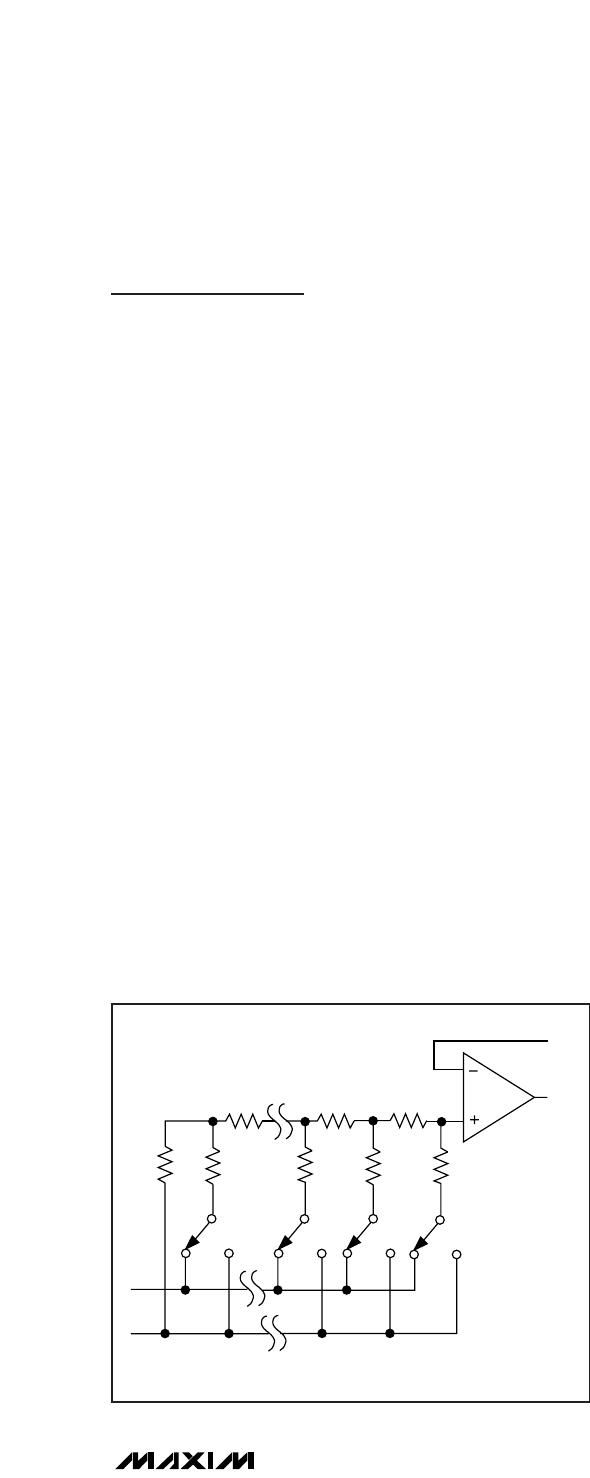
The DACs are inverted rail-to-rail ladder networks that
convert 12-bit digital inputs into equivalent analog out-
put voltages in proportion to the applied reference volt-
age inputs. DACs A and B share the REFAB input,
while DACs C and D share the REFCD input. The two
reference inputs allow different full-scale output voltage
ranges for each pair of DACs. Figure 1 shows a simpli-
fied circuit diagram of one of the four DACs.
Reference Inputs
The two reference inputs accept positive DC and AC
signals. The voltage at each reference input sets the
full-scale output voltage for the two corresponding
DACs. The reference input voltage range is 0V to (V
DD
- 1.4V). The output voltages (V
OUT_
) are represented by
a digitally programmable voltage source as:
V
OUT_
= (V
REF
x NB/4096) x Gain
where NB is the numeric value of the binary input code
(0 to 4095) of the DAC. V
REF
is the reference voltage.
Gain is the externally set voltage gain.
The impedance at each reference input is code-depen-
dent, ranging from a low value of 10k when both
DACs connected to the reference accept an input code
of 555 hex, to a high value exceeding giga-ohms with
an input code of 000 hex. The load regulation of the ref-
erence source affects the performance of the devices
as the input impedance at the reference inputs is code
dependent. The REFAB and REFCD reference inputs
provide a 10k guaranteed minimum input impedance.
When the same voltage source drives the two reference
inputs, the effective minimum impedance is 5k. A volt-
age reference with an excellent load regulation of
0.0002mV/mA, such as the MAX6033, is capable of dri-
ving both reference inputs simultaneously at 2.5V.
Driving REFAB and REFCD separately improves refer-
ence accuracy.
The REFAB and REFCD inputs enter a high-impedance
state, with a typical input leakage current of 0.02µA,
when the MAX5500/MAX5501 are in shutdown. The ref-
erence input capacitance is also code dependent and
typically ranges from 20pF with an input code of all 0s
to 100pF with an input code of all 1s.
Output Amplifiers
All DAC outputs are internally buffered by precision
amplifiers with a typical slew rate of 0.6V/µs. Access to
the inverting input of each output amplifier provides the
greater flexibility in output gain setting/signal condition-
ing (see the
Applications Information
section).
With a full-scale transition at the output, the typical set-
tling time to within ±0.5 LSB is 12µs when the output is
loaded with 5k in parallel with 100pF. A load of less
than 2k at the output degrades performance. See the
Typical Operating Characteristics
for the output dynamic
responses and settling performances of the amplifiers.
Power-Down Mode
The MAX5500/MAX5501 feature a software-program-
mable shutdown that reduces supply current to a typi-
cal value of 10µA. Drive PDL high to enable the
shutdown mode. Write 1100XXXXXXXXXXXX as the
input-control word to put the device in power-down
mode (Table 1).
In power-down mode, the output amplifiers and the ref-
erence inputs enter a high-impedance state.
The serial interface remains active. Data in the input
registers is retained in power-down, allowing the
devices to recall the output states prior to entering shut-
down. Start up from power-down either by recalling the
previous configuration or by updating the DACs with
new data. Allow 15µs for the outputs to stabilize when
powering up the devices or bringing the devices out of
shutdown.
OUT_
FB_
SHOWN FOR ALL 1s ON DAC
D0 D9 D10
D11
2R
2R 2R 2R 2R
RRR
REF_
AGND
Figure 1. Simplified DAC Circuit Diagram
MAX5500/MAX5501
Low-Power, Quad, 12-Bit
Voltage-Output DACs with Serial Interface
8 _______________________________________________________________________________________
SCLK
DIN
DOUT*
CS
SK
SO
SI*
I/O
MAX5500
MAX5501
MICROWIRE
PORT
*THE DOUT-SI CONNECTION IS NOT REQUIRED FOR WRITING TO THE
MAX5500/MAX5501, BUT CAN BE USED FOR READBACK PURPOSES.
Figure 2. Connections for MICROWIRE
Serial-Interface Configurations
The MAX5500/MAX5501s’ 3-wire serial interface is
compatible with both MICROWIRE (Figure 2) and
SPI/QSPI (Figure 3). The serial input word consists of
two address bits and two control bits followed by 12
data bits (MSB first), as shown in Figure 4. The 4-bit
address/control code determines the MAX5500/
MAX5501s’ response outlined in Table 1. The connec-
tion between DOUT and the serial-interface port is not
necessary, but may be used for data echo. Data held in
the shift register can be shifted out of DOUT and
returned to the µP for data verification.
The digital inputs of the MAX5500/MAX5501 are double
buffered. Depending on the command issued through the
serial interface, the input register(s) can be loaded without
affecting the DAC register(s), the DAC register(s) can be
loaded directly, or all four DAC registers can be updated
simultaneously from the input registers (Table 1).
Serial-Interface Description
The MAX5500/MAX5501 require 16 bits of serial data.
Table 1 lists the serial-interface programming com-
mands. For certain commands, the 12 data bits are
don’t-care bits. Data is sent MSB first and can be sent
in two 8-bit packets or one 16-bit word (CS must remain
low until 16 bits are transferred). The serial data is com-
posed of two DAC address bits (A1, A0) and two control
bits (C1, C0), followed by the 12 data bits D11–D0
(Figure 4). The 4-bit address/control code determines:
The register(s) to be updated
The clock edge on which data is to be clocked out
through the serial-data output (DOUT)
The state of the user-programmable logic output
(UPO)
If the device is to enter shutdown mode (assuming
PDL is high)
How the device is configured when exiting out of
shutdown mode
DOUT*
DIN
SCLK
CS
MISO*
MOSI
SCK
I/O
SPI/QSPI
PORT
SS
+5V
CPOL = 0, CPHA = 0
*THE DOUT-MISO CONNECTION IS NOT REQUIRED FOR WRITING TO THE
MAX5500/MAX5501, BUT CAN BE USED FOR READBACK PURPOSES.
MAX5500
MAX5501
Figure 3. Connections for SPI/QSPI
MSB.................................................................................................................................LSB
MSB...........................................................................................LSB
16 BITS OF SERIAL DATA
ADDRESS
BITS
CONTROL
BITS
DATA BITS
4 ADDRESS/
CONTROL BITS
D11..............................................................................................D0
A1 A0 C1 C0
12 DATA BITS
Figure 4. Serial-Data Format
MAX5500/MAX5501
16-BIT SERIAL WORD
A1 A0 C1 C0
D11................D0
MSB LSB
FUNCTION
0
0
1
1
0
1
0
1
0
0
0
0
1
1
1
1
12-bit DAC data
12-bit DAC data
12-bit DAC data
12-bit DAC data
Load input register A; DAC registers unchanged.
Load input register B; DAC registers unchanged.
Load input register C; DAC registers unchanged.
Load input register D; DAC registers unchanged.
0
0
1
1
0
1
0
1
1
1
1
1
1
1
1
1
12-bit DAC data
12-bit DAC data
12-bit DAC data
12-bit DAC data
Load input register A; all DAC registers updated.
Load input register B; all DAC registers updated.
Load input register C; all DAC registers updated.
Load input register D; all DAC registers updated.
0 1 0 0 XXXXXXXXXXXX Update all DAC registers from their respective input registers (startup).
1 0 0 0 12-bit DAC data Load all DAC registers from shift register (startup).
1 1 0 0 XXXXXXXXXXXX Shutdown (provided PDL = 1)
0 0 1 0 XXXXXXXXXXXX UPO goes low (default)
0 1 1 0 XXXXXXXXXXXX UPO goes high
0 0 0 0 XXXXXXXXXXXX No operation (NOP) to DAC registers
1 1 1 0 XXXXXXXXXXXX Mode 1, DOUT clocked out on SCLK’s rising edge. All DAC registers updated.
1 0 1 0 XXXXXXXXXXXX
Mode 0, DOUT clocked out on SCLK’s falling edge. All DAC registers updated
(default).
Table 1. Serial-Interface Programming Commands
Figure 5 shows the serial-interface timing requirements.
The CS input must be low to enable the DAC’s serial
interface. When CS is high, the interface control circuitry
is disabled. CS must go low for at least t
CSS
before the
rising serial clock (SCLK) edge to properly clock in the
first bit. When CS is low, data is clocked into the internal
shift register through the serial data input (DIN) on the
rising edge of SCLK. The maximum guaranteed clock
frequency is 10MHz. Data is latched into the appropriate
input/DAC registers on the rising edge of CS.
The programming command “load-all-dacs-from-shift-
register” allows all input and DAC registers to be simul-
taneously loaded with the same digital code from the
input shift register. The no operation (NOP) command
leaves the register contents unaffected. This feature is
used in a daisy-chain configuration (see the
Daisy
Chaining Devices
section).
The command to change the clock edge on which seri-
al data is shifted out of DOUT also loads data from all
input registers to their respective DAC registers.
Serial-Data Output (DOUT)
The serial-data output, DOUT, is the internal shift regis-
ter’s output. The MAX5500/MAX5501 can be pro-
grammed so that data is clocked out of DOUT on the
rising edge of SCLK (mode 1) or the falling edge (mode
0). In mode 0, output data at DOUT lags input data at
DIN by 16.5 clock cycles, maintaining compatibility with
MICROWIRE, SPI/QSPI, and other serial interfaces. In
mode 1, output data lags input data by 16 clock cycles.
On power-up, DOUT defaults to mode 0 timing.
User-Programmable Logic Output (UPO)
The user-programmable logic output, UPO, allows an
external device to be controlled through the
MAX5500/MAX5501 serial interface (Table 1).
Low-Power, Quad, 12-Bit
Voltage-Output DACs with Serial Interface
_______________________________________________________________________________________ 9

MAX5500AGAP+

Mfr. #:
Manufacturer:
Maxim Integrated
Description:
Digital to Analog Converters - DAC 12-Bit 4Ch Precision DAC
Lifecycle:
New from this manufacturer.
Delivery:
DHL FedEx Ups TNT EMS
Payment:
T/T Paypal Visa MoneyGram Western Union