LT5557
3
5557fc
Note 1: Stresses beyond those listed under Absolute Maximum Ratings may
cause permanent damage to the device. Exposure to any Absolute Maximum
Rating condition for extended periods may affect device reliability and lifetime.
Note 2: 450MHz and 900MHz performance measured with external LO
and RF matching. 2600MHz and 3600MHz performance measured with
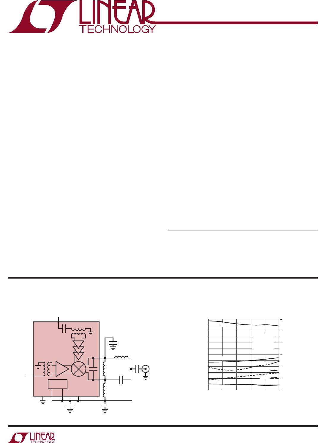
external RF matching. See Figure 1 and Applications Information.
Standard Downmixer Application: V
CC
= 3.3V, EN = High, T
A
= 25°C, P
RF
= –6dBm (–6dBm/tone for 2-tone IIP3 tests, ∆f = 1MHz), f
LO
= f
RF
– f
IF
, P
LO
= –3dBm (0dBm for 450MHz and 900MHz tests), IF output measured at 240MHz, unless otherwise noted. Test circuit
shown in Figure 1. (Notes 2, 3, 4)
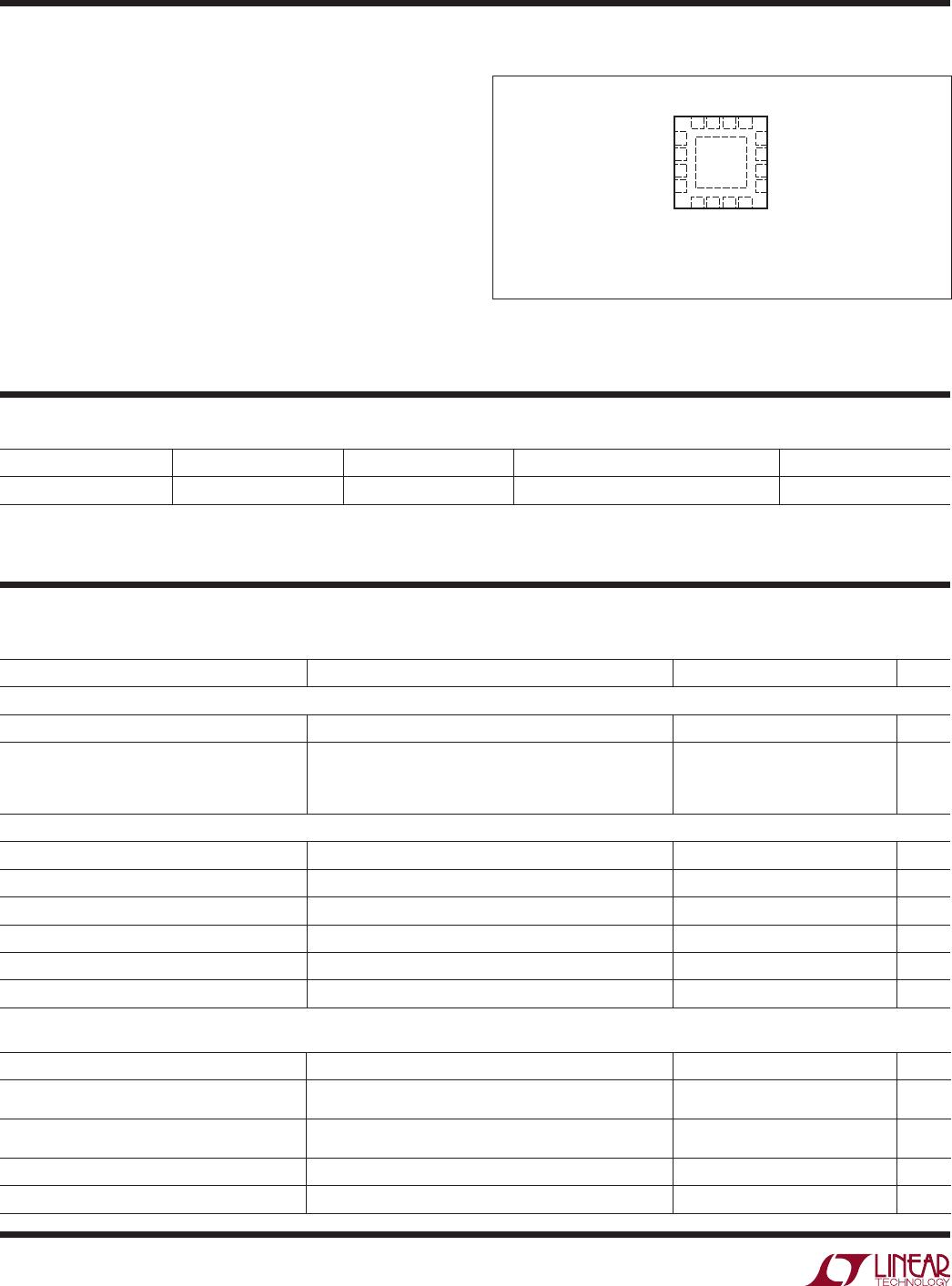
PARAMETER CONDITIONS MIN TYP MAX UNITS
Conversion Gain RF = 450MHz, IF = 70MHz, High Side LO
RF = 900MHz, IF = 140MHz
RF = 1750MHz
RF = 1950MHz
RF = 2150MHz
RF = 2600MHz, IF = 360MHz
RF = 3600MHz, IF = 450MHz
2.9
3.3
3.0
2.9
2.9
2.5
1.7
dB
dB
dB
dB
dB
dB
dB
Conversion Gain vs Temperature T
A
= –40°C to 85°C, RF = 1950MHz –0.0217 dB/°C
Input 3rd Order Intercept RF = 450MHz, IF = 70MHz, High Side LO
RF = 900MHz, IF = 140MHz
RF = 1750MHz
RF = 1950MHz
RF = 2150MHz
RF = 2600MHz, IF = 360MHz
RF = 3600MHz, IF = 450MHz
24.1
25.6
25.5
24.7
24.3
23.7
23.5
dBm
dBm
dBm
dBm
dBm
dBm
dBm
Single-Sideband Noise Figure RF = 450MHz, IF = 70MHz, High Side LO
RF = 900MHz, IF = 140MHz
RF = 1750MHz
RF = 1950MHz
RF = 2150MHz
RF = 2600MHz, IF = 360MHz
RF = 3600MHz, IF = 450MHz
12.7
10.6
11.3
11.7
12.8
13.2
15.4
dB
dB
dB
dB
dB
dB
dB
LO to RF Leakage f
LO
= 380MHz to 1600MHz
f
LO
= 1600MHz to 4000MHz
≤–50
≤–45
dBm
dBm
LO to IF Leakage f
LO
= 380MHz to 2200MHz
f
LO
= 2200MHz to 4000MHz
≤–42
≤–38
dBm
dBm
RF to LO Isolation f
RF
= 400MHz to 1700MHz
f
RF
= 1700MHz to 3800MHz
>50
>42
dB
dB
RF to IF Isolation f
RF
= 400MHz to 2300MHz
f
RF
= 2300MHz to 3800MHz
>41
>37
dB
dB
2RF-2LO Output Spurious Product
(f
RF
= f
LO
+ f
IF
/2)
900MHz: f
RF
= 830MHz at –6dBm, f
IF
= 140MHz
1950MHz: f
RF
= 1830MHz at –6dBm, f
IF
= 240MHz
–61
–53
dBc
dBc
3RF-3LO Output Spurious Product
(f
RF
= f
LO
+ f
IF
/3)
900MHz: f
RF
= 806.67MHz at –6dBm, f
IF
= 140MHz
1950MHz: f
RF
= 1790MHz at –6dBm, f
IF
= 240MHz
–83
–70
dBc
dBc
Input 1dB Compression RF = 450MHz, IF = 70MHz, High Side LO
RF = 900MHz, IF = 140MHz
RF = 1950MHz
RF = 2600MHz, IF = 360MHz
RF = 3600MHz, IF = 450MHz
10.0
8.8
8.8
8.6
9.1
dBm
dBm
dBm
dBm
dBm
Note 3: The LT5557 is guaranteed functional over the –40°C to 85°C
operating temperature range.
Note 4: SSB Noise Figure measurements performed with a small-signal
noise source and bandpass filter on RF input, and no other RF signal
applied.
ac elecTrical characTerisTics
PARAMETER CONDITIONS MIN TYP MAX UNITS
LO Input Return Loss Z
O
= 50Ω, 1000MHz to 5000MHz (No External Matching) >10 dB
IF Output Impedance Differential at 240MHz 529Ω||2.6pF R||C
LO Input Power 1200MHz to 4200MHz
380MHz to 1200MHz
–8
–5
–3
0
2
5
dBm
dBm
Test circuit shown in Figure 1. (Notes 2, 3)