LT5557
9
5557fc
applicaTions inForMaTion
Introduction
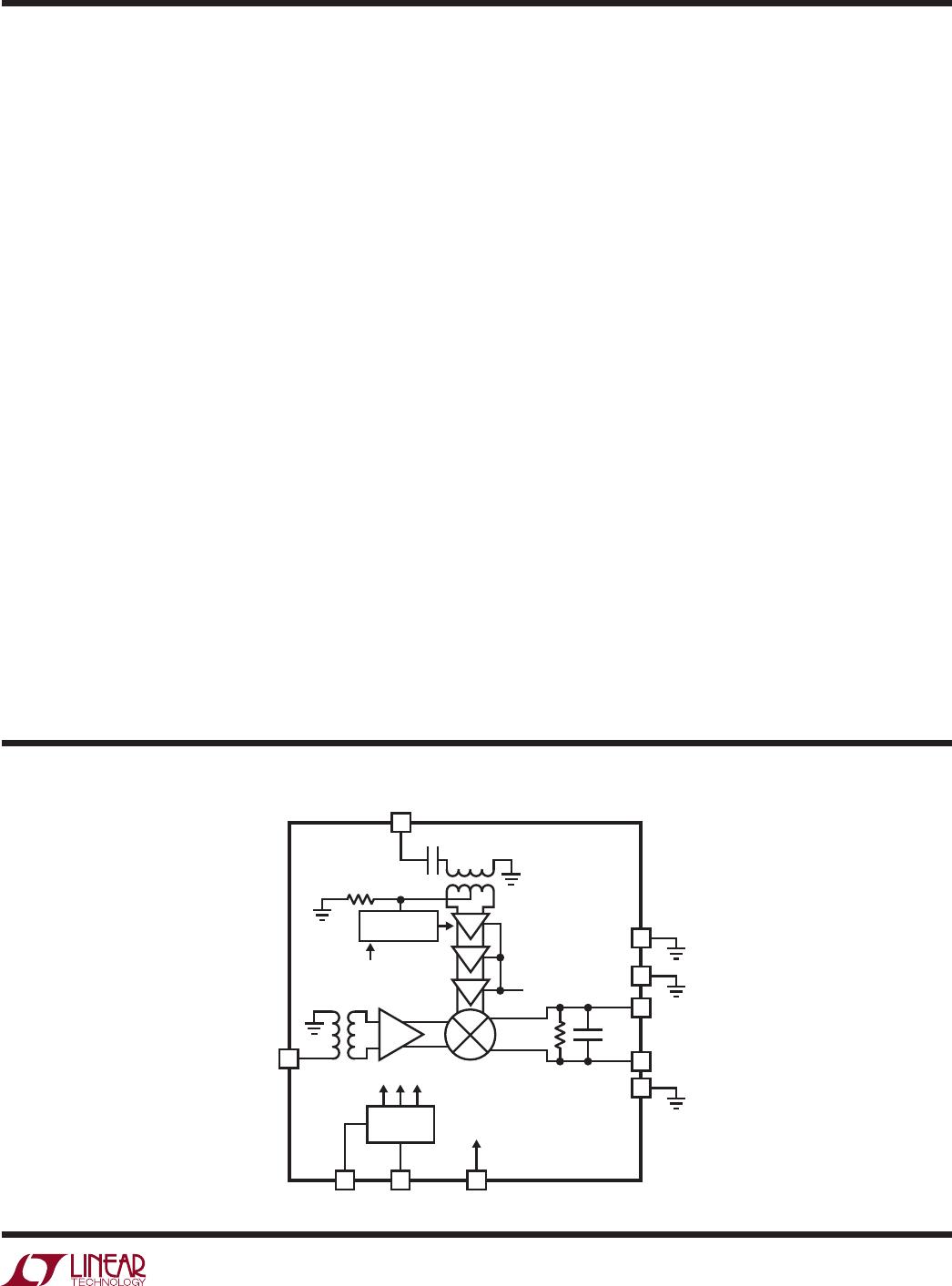
The LT5557 consists of a high linearity double-balanced
mixer, RF buffer amplifier, high speed limiting LO buffer
amplifier and bias/enable circuits. The RF and LO inputs
are both single ended. The IF output is differential. Low
side or high side LO injection can be used.
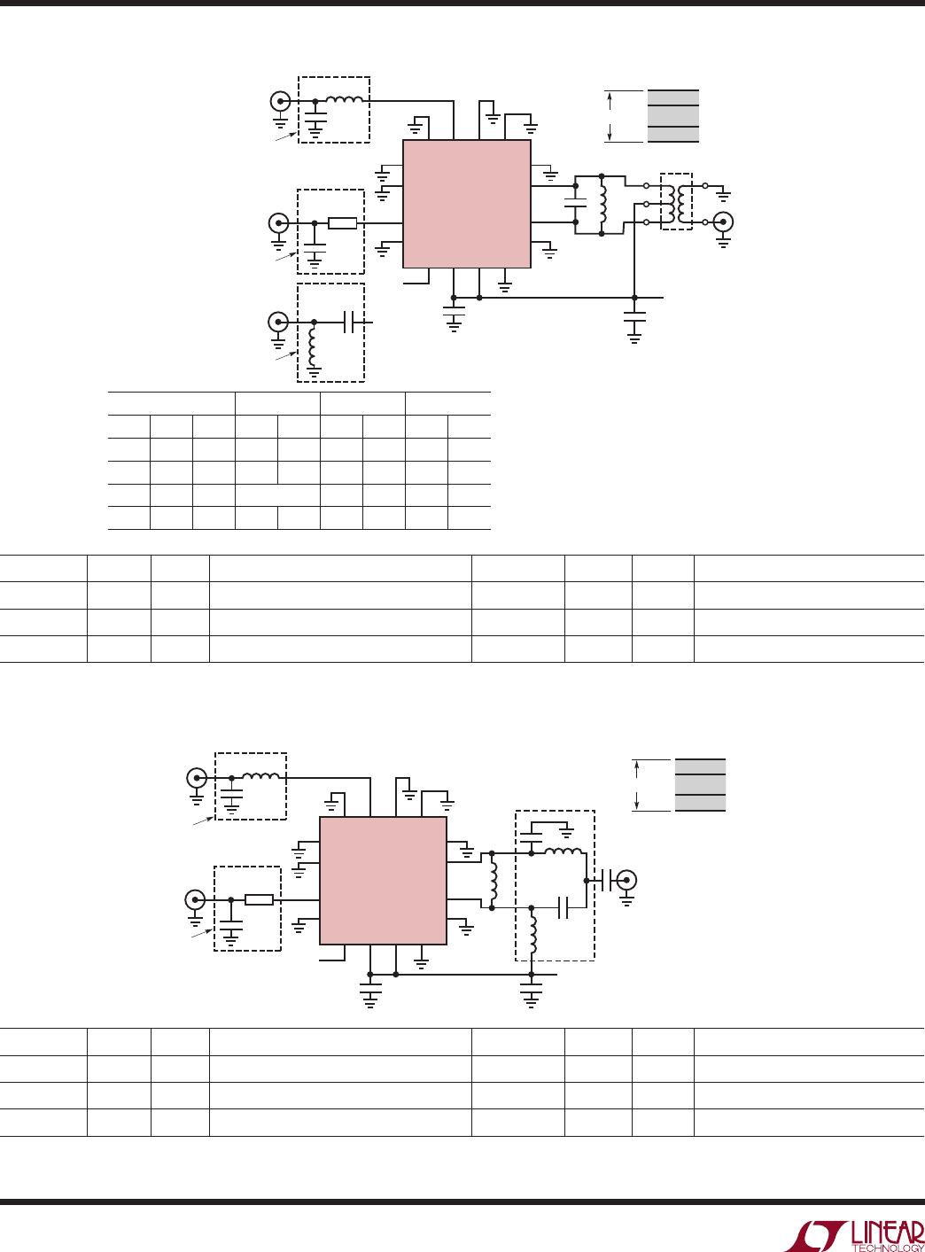
Two evaluation circuits are available. The standard evalua-
tion circuit, shown in Figure 1, incorporates transformer-
based IF matching and is intended for applications that
require the highest dynamic range and the widest IF
bandwidth. The second evaluation circuit, shown in Fig-
ure 2, replaces the IF transformer with a discrete IF balun
for reduced solution cost and size. The discrete IF balun
delivers higher conversion gain, but slightly degraded IIP3
and noise figure, and reduced IF bandwidth.
RF Input Port
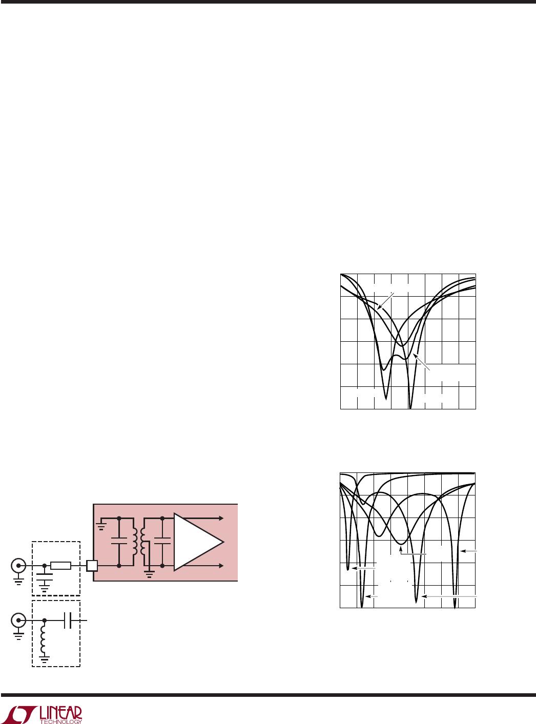
The mixer’s RF input, shown in Figure 3, consists of an
integrated transformer and a high linearity differential
amplifier. The primary terminals of the transformer are
connected to the RF input (Pin 3) and ground. The sec-
ondary side of the transformer is internally connected to
the amplifier’s differential inputs. The DC resistance of the
primary is 4.2Ω. If the RF source has DC voltage present,
then a coupling capacitor must be used in series with
the RF input pin.
The RF input is internally matched from 1.6GHz to 2.3GHz,
requiring no external components over this frequency
range. The input return loss, shown in Figure 4a, is typi-
cally 12dB at the band edges. The input match at the lower
band edge can be optimized with a series 3.9pF capacitor
at Pin 3, which improves the 1.6GHz return loss to greater
than 25dB. Likewise, the 2.3GHz match can be improved
to greater than 25dB with a series 1.5nH inductor. A
series 2.7nH/2.2pF network will simultaneously optimize
the lower and upper band edges and expand the RF input
bandwidth to 1.2GHz-2.5GHz. Measured RF input return
losses for these three cases are also plotted in Figure 4a.
Alternatively, the input match can be shifted as low as
400MHz or up to 3800MHz by adding a shunt capacitor
(C5) to the RF input. A 450MHz input match is realized with
C5 = 12pF, located 6.5mm away from Pin 3 on the evalua-
tion board’s 50Ω input transmission line. A 900MHz input
match requires C5 = 3.9pF, located at 1.7mm. A 3.6GHz
input match is realized with C5 = 1pF, located at 2.9mm.
Figure 3. RF Input Schematic
(4a) Series Reactance Matching
(4b) Series Shunt Matching
Figure 4. RF Input Return Loss with
and without External Matching
RF
IN
Z
O
=
50Ω
L = L (mm)
C5
RF
5557 F03
RF
IN
C5
L5
LOWPASS MATCH
FOR 450MHz, 900MHz
and 3.6GHz RF
HIGHPASS MATCH
FOR 2.6GHz RF
AND WIDEBAND RF
TO
MIXER
3
FREQUENCY (GHz)
0.2
–30
RF PORT RETURN LOSS (dB)
–25
–20
–15
–10
1.2 2.2
3.2
4.2
5557 F04a
–5
0
0.7 1.7
2.7
3.7
SERIES 2.7nH
AND 2.2pF
NO EXT MATCH
SERIES 1.5nH
SERIES 3.9pF
FREQUENCY (GHz)
0.2
–30
RF PORT RETURN LOSS (dB)
–25
–20
–15
–10
1.2 2.2
3.2
4.2
5557 F04b
–5
0
0.7 1.7
2.7
3.7
450MHz
L = 6.5mm
C5 = 12pF
2.6GHz
SERIES 3.9pF
SHUNT 3.6nH
3.6GHz
L = 2.9mm
C5 = 1pF
900MHz
L = 1.7mm
C5 = 3.9pF
NO EXT
MATCH