LT5557
10
5557fc
applicaTions inForMaTion
This series transmission line/shunt capacitor matching to-
pology allows the LT5557 to be used for multiple frequency
standards without circuit board layout modifications. The
series transmission line can also be replaced with a series
chip inductor for a more compact layout.
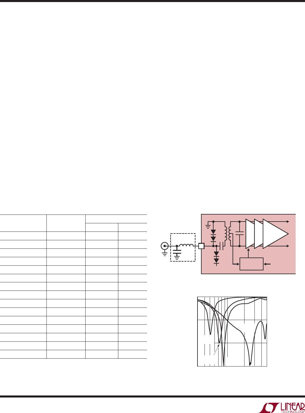
Input return losses for the 450MHz, 900MHz, 2.6GHz
and 3.6GHz applications are plotted in Figure 4b. The
input return loss with no external matching is repeated
in Figure 4b for comparison. The 2.6GHz RF input match
uses the highpass matching network shown in Figures 1
and 3 with C5 = 3.9pF and L5 = 3.6nH. The highpass in-
put matching network is also used to create a wideband
or dual-band input match. For example, with C5 = 3.3pF
and L5 = 10nH, the RF input is matched from 800MHz to
2.2GHz, with optimum matching in the 800MHz to 1.1GHz
and 1.6GHz to 2.2GHz bands, simultaneously.
RF input impedance and S11 versus frequency (with no
external matching) are listed in Table 1 and referenced
to Pin 3. The S11 data can be used with a microwave
circuit simulator to design custom matching networks
and simulate board level interfacing to the RF input filter.
Table 1. RF Input Impedance vs Frequency
FREQUENCY
(MHz)
INPUT
IMPEDANCE
S11
MAG ANGLE
50 4.6 + j2.3 0.832 174.7
300 9.1 + j11.2 0.706 153.8
450 12.0 + j14.5 0.639 145.8
600 14.7 + j17.4 0.588 138.7
900 20.5 + j23.3 0.506 123.4
1300 34.4 + j30.3 0.380 97.5
1700 59.6 + j23.8 0.229 55.8
1950 69.2 + j2.8 0.163 6.9
2200 59.2 – j18.1 0.184 –53.5
2450 41.5 – j24.5 0.274 –94.2
2700 28.3 – j21.3 0.374 –120.3
3000 19.0 – j13.5 0.481 –145.5
3300 13.9 – j5.1 0.568 –167.3
3600 10.8 + j3.4 0.645 171.9
3900 9.4 + j12.3 0.700 151.4
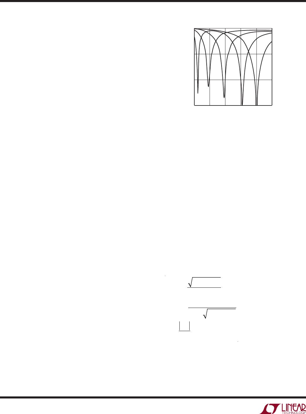
LO Input Port
The mixers LO input, shown in Figure 5, consists of an
integrated transformer and high speed limiting differential
amplifiers. The amplifiers are designed to precisely drive
the mixer for the highest linearity and the lowest noise
figure. An internal DC blocking capacitor in series with the
transformers primary eliminates the need for an external
blocking capacitor.
The LO input is internally matched from 1GHz to 5GHz.
The input match can be shifted down, as low as 750MHz,
with a single shunt capacitor (C4) on Pin 15. One exam-
ple is plotted in Figure 6 where C4 = 2.7pF produces a
750MHz to 1GHz match.
LO input matching below 750MHz requires the series
inductor (L4)/shunt capacitor (C4) network shown in
Figure 5. Two examples are plotted in Figure 6, where L4
= 2.7nH/C4 = 3.9pF produces a 650MHz to 830MHz match
and L4 = 10nH/C4 = 8.2pF produces a 460MHz to 560MHz
match. The evaluation boards do not include pads for L4,
so the circuit trace needs to be cut near Pin 15 to insert
L4. A low cost multilayer chip inductor is adequate for L4.
Figure 5. LO Input Schematic
Figure 6. LO Input Return Loss
LO
IN
C4
L4
LO
V
CC2
LIMITER
V
REF
5557 F05
EXTERNAL
MATCHING
FOR LO < 1GHz
TO
MIXER
15
REGULATOR
LO FREQUENCY (GHz)
0.3
L4 = 10nH
C4 = 8.2pF
L4 = 2.7nH
C4 = 3.9pF
L4 = 0
C4 = 2.7pF
–30
LO PORT RETURN LOSS (dB)
–10
0
1 5
5557 G06
–20
NO EXT
MATCH
LT5557
11
5557fc
applicaTions inForMaTion
The optimum LO drive is –3dBm for LO frequencies above
1.2GHz, although the amplifiers are designed to accom-
modate several dB of LO input power variation without
significant mixer performance variation. Below 1.2GHz,
0dBm LO drive is recommended for optimum noise figure,
although –3dBm will still deliver good conversion gain
and linearity.
Custom matching networks can be designed using the port
impedance data listed in Table 2. This data is referenced
to the LO pin with no external matching.
Table 2. LO Input Impedance vs Frequency
FREQUENCY
(MHz)
INPUT
IMPEDANCE
S11
MAG ANGLE
50 10.0 – j326 0.991 –17.4
300 8.5 – j41.9 0.820 –99.2
500 11.8 – j10.1 0.632 –155.9
700 18.8 + j10.9 0.474 151.8
900 35.0 + j27.4 0.350 100.8
1200 72.9 + j19.3 0.241 31.3
1500 70.0 – j12.6 0.196 –26.1
1800 55.0 – j17.0 0.167 –64.3
2200 47.8 – j9.7 0.102 –97.2
2600 53.6 – j1.9 0.039 –26.8
3000 66.7 + j0.7 0.143 2.1
3500 82.1 – j13.9 0.263 –17.4
4000 69.0 – j30.1 0.290 –43.5
4500 43.7 – j13.2 0.154 –107.5
5000 36.4 + j19.8 0.271 111.6
IF Output Port
The IF outputs, IF
+
and IF
, are internally connected to the
collectors of the mixer switching transistors (see Figure 7).
Both pins must be biased at the supply voltage, which
can be applied through the center tap of a transformer or
through matching inductors. Each IF pin draws 26.6mA
of supply current (53.2mA total). For optimum single-
ended performance, these differential outputs should
be combined externally through an IF transformer or a
discrete IF balun circuit. The standard evaluation board
(see Figure 1) includes an IF transformer for impedance
transformation and differential to single-ended transfor-
mation. A second evaluation board (see Figure 2) realizes
the same functionality with a discrete IF balun circuit.
The IF output impedance can be modeled as 560Ω in
parallel with 2.6pF at low frequencies. An equivalent small-
signal model (including bondwire inductance) is shown
in Figure 8. Frequency-dependent differential IF output
impedance is listed in Table 3. This data is referenced
to the package pins (with no external components) and
includes the effects of IC and package parasitics. The IF
output can be matched for IF frequencies as low as several
kHz or as high as 600MHz.
Table 3. IF Output Impedance vs Frequency
FREQUENCY (MHz)
DIFFERENTIAL OUTPUT
IMPEDANCE (R
IF
|| X
IF
)
1 560 || – j63.7k (2.6pF)
70 556 || – j870 (2.6pF)
140 551 || – j440 (2.6pF)
190 523 || – j320 (2.6pF)
240 529 || – j254 (2.6pF)
300 509 || – j200 (2.66pF)
360 483 || – j163 (2.7pF)
450 448 || – j125 (2.83pF)
600 396 || – j92 (2.88pF)
Two methods of differential to single-ended IF matching
are described:
• Transformer-basedbandpass
• DiscreteIFbalun
Figure 7. IF Output with External Matching
Figure 8. IF Output Small-Signal Model
11
10
IF
+
L1
8:1
5557 F07
IF
V
CC
C3
V
CC
IF
OUT
50Ω
11
10
IF
+
0.7nH
0.7nH
5557 F08
IF
R
S
C
S
R
IF
|| X
IF
LT5557
12
5557fc
applicaTions inForMaTion
Transformer-Based Bandpass IF Matching
The standard evaluation board (shown in Figure 1) uses
an L-C bandpass IF matching network, with an 8:1 trans-
former connected across the IF pins. The L-C network
maximizes mixer performance at the desired IF frequency.
The transformer performs impedance transformation and
provides a single-ended 50Ω output.
The value of L1 is calculated as:
L1 = 1/[(2πf
IF
)
2
•C
IF
]
where C
IF
is the sum of C3 and the internal IF capacitance
(listed in Table 3). The value of C3 is selected such that L1
falls on a standard value, while satisfying the desired IF
bandwidth. The IF bandwidth can be estimated as:
BW
IF
= 1/(2πR
EFF
C
IF
)
where R
EFF
, the effective IF resistance when loaded with
the transformer and inductor loss, is approximately 200Ω.
Below 40MHz, the magnitude of the internal IF reactance
is relatively high compared to the internal resistance. In
this case, L1 (and C3) can be eliminated, and the 8:1
transformer alone is adequate for IF matching.
The LT5557 was characterized with IF frequencies of
70MHz, 140MHz, 240MHz, 360MHz and 450MHz. The
values of L1 and C3 used for these frequencies are tabu-
lated in Figure 1 and repeated in Figure 9. In all cases,
L1 is a high-Q 0603 wire-wound chip inductor, for high-
est conversion gain. Low cost multilayer chip inductors
can be substituted, with a slight reduction in conversion
gain. The measured IF output return losses are plotted in
Figure 9.
Discrete IF Balun Matching
For many applications, it is possible to replace the IF
transformer with the discrete IF balun shown in Figure 2.
The values of L1, L2, C6 and C7 are calculated to realize
a 180 degree phase shift at the desired IF frequency and
provide a 50Ω single-ended output, using the following
equations. Inductor L3 is calculated to cancel the internal
2.6pF capacitance. L3 also supplies bias voltage to the IF
+
pin. Low cost multilayer chip inductors are adequate for
L1, L2 and L3. C3 is a DC blocking capacitor.
L1, L2 =
R
IF
R
OUT
ω
IF
C6,C7 =
1
ω
IF
R
IF
R
OUT
L3 =
X
IF
ω
IF
Figure 9. IF Output Return Loss with
Transformer-Based Bandpass Matching
IF FREQUENCY (MHz)
50
A: 70MHz, L1 = 270nH, C3 = 15pF
B: 140MHz, L1 = 180nH, C3 = 3.9pF
C: 240MHz, L1 = 82nH, C3 = 2.2pF
D: 360MHz, L1 = 47nH, C3 = 1.2pF
E: 450MHz, L1 = 39nH, C3 = 0pF
–30
IF PORT RETURN LOSS (dB0
–20
–10
0
150 250 350 450
5557 G09
550
A
B
C
D E

LT5557EUF#TRPBF

Mfr. #:
Manufacturer:
Analog Devices Inc.
Description:
RF Mixer 400 MHz to 3.8 GHz 3.3V Downconverting Mixer
Lifecycle:
New from this manufacturer.
Delivery:
DHL FedEx Ups TNT EMS
Payment:
T/T Paypal Visa MoneyGram Western Union

Products related to this Datasheet