LT5557
13
5557fc
applicaTions inForMaTion
These equations give a good starting point, but it is usually
necessary to adjust the component values after building
and testing the circuit. The final solution can be achieved
with less iteration by considering the parasitics of L3 in
the above calculations. Specifically, the effective parallel
resistance of L3 (calculated from the manufacturer’s Q
data) will reduce the value of R
IF
, which in turn influ-
ences the calculated values of L1 (= L2) and C6 (= C7).
Also, the effective parallel capacitance of L3 (taken from
the manufacturers SRF data) must be considered, since
it is in parallel with X
IF
(from Table 3). Frequently, the
calculated value for L1 does not fall on a standard value
for the desired IF. In this case, a simple solution is to load
the IF output with a high value external chip resistor in
parallel with L3, which reduces the value of R
IF
, until L1
is a standard value.
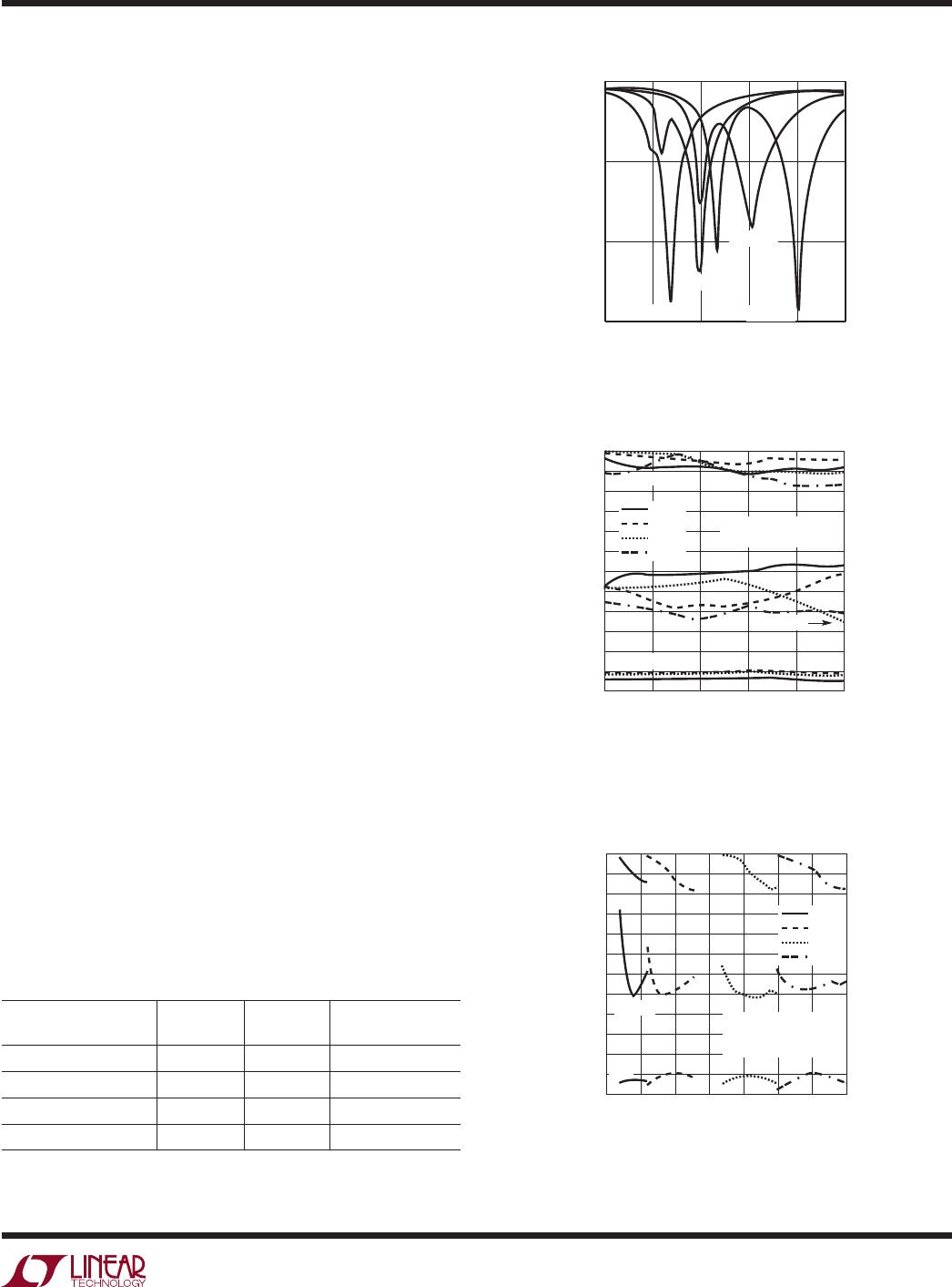
Discrete IF balun element values for four common IF fre-
quencies (190MHz, 240MHz, 360MHz and 450MHz) are
listed in Table 4. The 190MHz application circuit uses a
3.3k resistor in parallel with L3 as previously described.
The corresponding measured IF output return losses are
shown in Figure 10. Typical conversion gain, IIP3 and LO-IF
leakage, versus RF input frequency for all four examples is
shown in Figure 11. Typical conversion gain, IIP3 and noise
figure versus IF output frequency is shown in Figure 12.
Compared to the transformer-based IF matching technique,
this network delivers approximately 1dB higher conver-
sion gain (since the IF transformer loss is eliminated),
though noise figure and IIP3 are degraded slightly. The
most significant performance difference, as shown in
Figure 12, is the limited IF bandwidth available from the
discrete approach. For low IF frequencies, the absolute
bandwidth is small, whereas higher IF frequencies offer
wider bandwidth.
Table 5. Discrete IF Balun Element Values (R
OUT
= 50Ω)
IF FREQUENCY
(MHz)
L1, L2
C6, C7
L3
190 120nH 6.0pF 270nH || 3.3kΩ
240 100nH 4.7pF 150nH
360 56nH 3.0pF 82nH
450 47nH 2.2pF 47nH
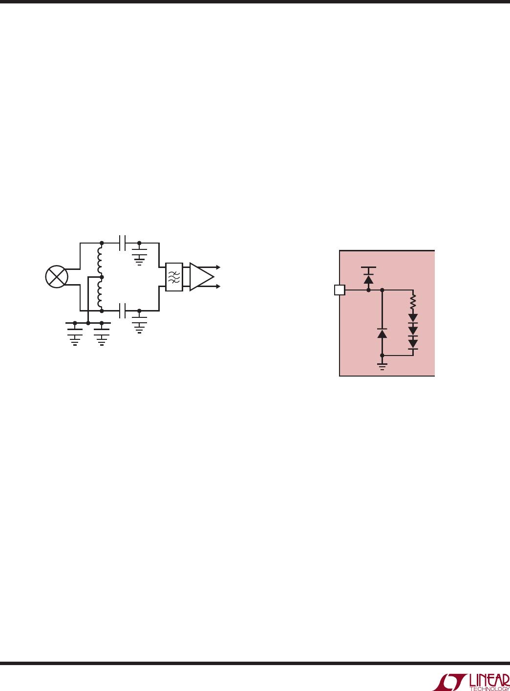
Differential IF Output Matching
Figure 10. IF Output Return Losses with Discrete Balun Matching
Figure 11. Conversion Gain, IIP3 and LO-IF Leakage
vs RF Input Frequency and IF Output Frequency
(in MHz) Using Discrete IF Balun Matching
Figure 12. Conversion Gain, IIP3 and SSB NF vs IF Output
Frequency Using Discrete IF Balun Matching
IF FREQUENCY (MHz)
50
–30
IF PORT RETURN LOSS (dB)
–20
–10
0
150 250 350 450
5557 F10
550
190 MHz
240 MHz
360 MHz
450 MHz
RF INPUT FREQUENCY (MHz)
1700
G
C
(dB), IIP3 (dBm)
LO-IF LEAKAGE (dBm)
8
22
24
26
1900
2100
4
18
14
12
6
20
2
16
10
–60
–10
–30
–40
–20
–70
–50
1800
2000
2200
LOW SIDE LO (–3dBm)
T
A
= 25°C
LO-IF
IIP3
G
C
190IF
240IF
360IF
450IF
IF OUTPUT FREQUENCY (MHz)
150
G
C
(dB), NF (dB), IIP3 (dBm)
10
22
24
26
250
350
400
5557 F12
6
18
14
8
20
2
4
16
12
200
300
450
500
RF = 1950MHz
LOW SIDE LO (–3dBm)
T
A
= 25°C
SSB NF
IIP3
G
C
190IF
240IF
360IF
450IF