Table 9: Single-Ended Output Slew Rate
For R
ON
= R
ZQ
/7
Parameter Symbol
DDR4-1333 / 1866 / 2133 / 2400 /2666
UnitMin Max
Single-ended output slew rate SRQ
se
2 7 V/ns
Notes:
1. SR = slew rate; Q = query output; se = single-ended signals
2. In two cases a maximum slew rate of 12V/ns applies for a single DQ signal within a byte
lane:
• Case 1 is defined for a single DQ signal within a byte lane that is switching into a cer-
tain direction (either from HIGH-to-LOW or LOW-to-HIGH) while all remaining DQ sig-
nals in the same byte lane are static (they stay at either HIGH or LOW).
• Case 2 is defined for a single DQ signal within a byte lane that is switching into a cer-
tain direction (either from HIGH-to-LOW or LOW-to-HIGH) while all remaining DQ sig-
nals in the same byte lane are switching into the opposite direction (from LOW-to-
HIGH or HIGH-to-LOW, respectively). For the remaining DQ signal switching into the
opposite direction, the standard maximum limit of 7 V/ns applies.
Differential Outputs
Table 10: Differential Output Levels
Parameter Symbol DDR4-1600 to DDR4-3200 Unit
AC differential output high measurement level (for output slew
rate)
V
OH,diff(AC)
0.3 × V
DDQ
V
AC differential output low measurement level (for output slew
rate)
V
OL,diff(AC)
–0.3 × V
DDQ
V
Note:
1. The swing of ±0.3 × V
DDQ
is based on approximately 50% of the static single-ended out-
put peak-to-peak swing with a driver impedance of RZQ/7 and an effective test load of
50Ω to V
TT
= V
DDQ
at each differential output.
Using the same reference load used for timing measurements, output slew rate for fall-
ing and rising edges is defined and measured between V
OL,diff(AC)
and V
OH,diff(AC)
for dif-
ferential signals.
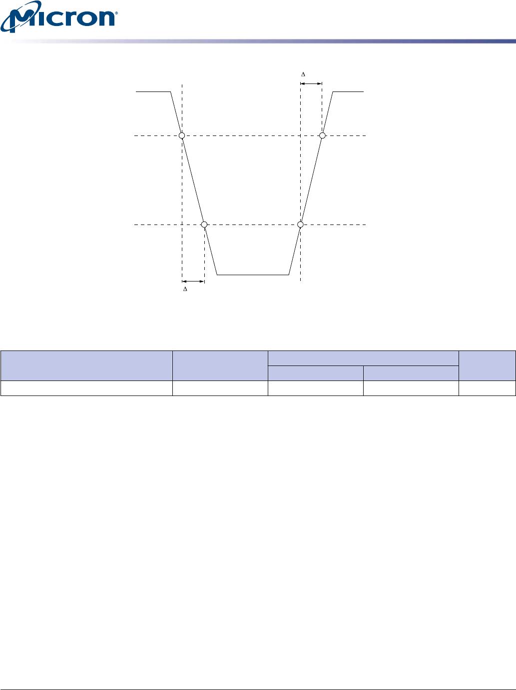
Table 11: Differential Output Slew Rate Definition
Description
Measured
Defined byFrom To
Differential output slew rate for rising edge V
OL,diff(AC)
V
OH,diff(AC)
[V
OH,diff(AC)
- V
OL,diff(AC)
]/ΔTR
diff
Differential output slew rate for falling edge V
OH,diff(AC)
V
OL,diff(AC)
[V
OH,diff(AC)
- V
OL,diff(AC)
]/ΔTF
diff
16Gb: x4, x8 TwinDie DDR4 SDRAM
Electrical Characteristics – AC and DC Output Measurement
Levels
PDF: 09005aef85fd40a1
DDR4_16Gb_x4_x8_2CS_TwinDie.pdf - Rev. D 12/16 EN
13
Micron Technology, Inc. reserves the right to change products or specifications without notice.
© 2015 Micron Technology, Inc. All rights reserved.