Functional Description
The TwinDie DDR4 SDRAM is a high-speed, CMOS dynamic random access memory
device internally configured as two 16-bank DDR4 SDRAM devices.
Although each die is tested individually within the dual-die package, some TwinDie test
results may vary from a like-die tested within a monolithic die package.
The DDR4 SDRAM uses a double data rate architecture to achieve high-speed opera-
tion. The double data rate architecture is an 8n-prefetch architecture with an interface
designed to transfer two data words per clock cycle at the I/O balls. A single read or
write access consists of a single 8n-bit-wide, one-clock-cycle data transfer at the inter-
nal DRAM core and eight corresponding n-bit-wide, one-half-clock-cycle data transfers
at the I/O balls.
The differential data strobe (DQS, DQS#) is transmitted externally, along with data, for
use in data capture at the DDR4 SDRAM input receiver. DQS is center-aligned with data
for WRITEs. The read data is transmitted by the DDR4 SDRAM and edge-aligned to the
data strobes.
Read and write accesses to the DDR4 SDRAM are burst-oriented. Accesses start at a se-
lected location and continue for a programmed number of locations in a programmed
sequence. Operation begins with the registration of an ACTIVATE command, which is
then followed by a READ or WRITE command. The address bits registered coincident
with the ACTIVATE command are used to select the bank and row to be accessed. The
address bits (including CSn#, BAn, and An) registered coincident with the READ or
WRITE command are used to select the rank, bank, and starting column location for the
burst access.
This data sheet provides a general description, package dimensions, and the package
ballout. Refer to the Micron monolithic DDR4 data sheet for complete information re-
garding individual die initialization, register definition, command descriptions, and die
operation.
Industrial Temperature
The industrial temperature (IT) option, if offered, requires that the case temperature
not exceed –40°C or 95°C. JEDEC specifications require the refresh rate to double when
T
C
exceeds 85°C; this also requires use of the high-temperature self refresh option. Addi-
tionally, ODT resistance, I
DD
values, some I
DD
specifications and the input/output im-
pedance must be derated when T
C
is < 0°C or > 95°C. See the DDR4 monolithic data
sheet for details.
16Gb: x4, x8 TwinDie DDR4 SDRAM
Functional Description
PDF: 09005aef85fd40a1
DDR4_16Gb_x4_x8_2CS_TwinDie.pdf - Rev. D 12/16 EN
7
Micron Technology, Inc. reserves the right to change products or specifications without notice.
© 2015 Micron Technology, Inc. All rights reserved.
Functional Block Diagrams
Figure 2: Functional Block Diagram (128 Meg x 4 x 16 Banks x 2 Ranks)
PAR
TEN
RESET
CK
CK#
DQ[3:0]
DQS, DQS#
DM
A[13:0],
ACT_n,
WE_n/A14,
CAS_n/A15,
RAS_n/A16,
BA[1:0],
BG[1:0]
CS0#
CKE0
ODT0
Rank 0
(128 Meg x 4 x 16 banks)
Rank 1
(128 Meg x 4 x 16 banks)
CS1#
CKE1
ODT1
ALERT_n
ZQ
Figure 3: Functional Block Diagram (64 Meg x 8 x 16 Banks x 2 Ranks)
TDQS#
TEN
PAR
RESET
CK
CK#
DQ[7:0]
DQS, DQS#
DBI/DM/TDQS
A[13:0],
ACT_n,
WE_n/A14,
CAS_n/A15,
RAS_n/A16,
BA[1:0],
BG[1:0]
CS0#
CKE0
ODT0
CS1#
CKE1
ODT1
ZQ
ALERT_n
Rank 1
(64 Meg x 8 x 16 banks)
Rank 0
(64 Meg x 8 x 16 banks)
16Gb: x4, x8 TwinDie DDR4 SDRAM
Functional Block Diagrams
PDF: 09005aef85fd40a1
DDR4_16Gb_x4_x8_2CS_TwinDie.pdf - Rev. D 12/16 EN
8
Micron Technology, Inc. reserves the right to change products or specifications without notice.
© 2015 Micron Technology, Inc. All rights reserved.
Electrical Specifications – Leakages
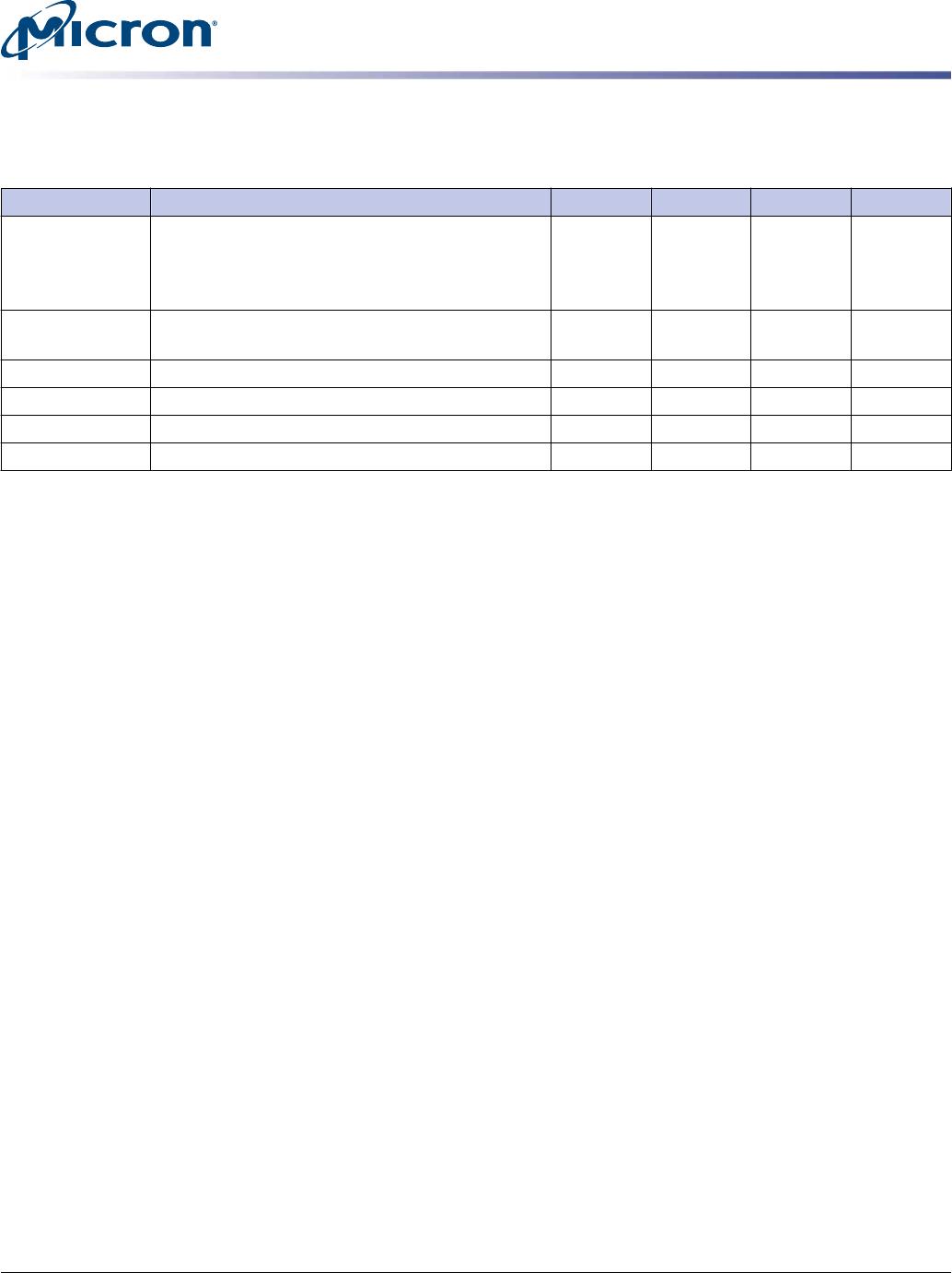
Table 4: Input and Output Leakages
Symbol Parameter Min Max Units Notes
I
IN
Input leakage current
Any input 0V V
IN
V
DD
,
V
REF
pin 0V V
IN
1.1V
(All other pins not under test = 0V)
–4 4 µA 1
I
VREFCA
V
REF
supply leakage current
(All other pins not under test = 0V)
–4 4 µA 2
I
ZQ
Input leakage on ZQ pin –6 6 µA
I
TEN
Input leakage on TEN pin –8 8 µA
I
OZpd
Output leakage: V
OUT
= V
DDQ
10 µA 3
I
OZpu
Output leakage: V
OUT
= V
SSQ
–100 µA 3, 4
Notes:
1. Any input 0V < V
IN
< 1.1V
2. V
REFCA
= V
DD
/2, V
DD
at valid level.
3. DQ are disabled.
4. ODT is disabled with the ODT input HIGH.
Temperature and Thermal Impedance
It is imperative that the DDR4 SDRAM device’s temperature specifications, shown in
the following table, be maintained in order to ensure the junction temperature is in the
proper operating range to meet data sheet specifications. An important step in main-
taining the proper junction temperature is using the device’s thermal impedances cor-
rectly. The thermal impedances listed in Table 6 (page 10) apply to the current die re-
vision and packages.
Incorrectly using thermal impedances can produce significant errors. Read Micron
technical note TN-00-08, “Thermal Applications,” prior to using the values listed in the
thermal impedance table. For designs that are expected to last several years and require
the flexibility to use several DRAM die shrinks, consider using final target theta values
(rather than existing values) to account for increased thermal impedances from the die
size reduction.
The DDR4 SDRAM device’s safe junction temperature range can be maintained when
the T
C
specification is not exceeded. In applications where the device’s ambient tem-
perature is too high, use of forced air and/or heat sinks may be required to satisfy the
case temperature specifications.
16Gb: x4, x8 TwinDie DDR4 SDRAM
Electrical Specifications – Leakages
PDF: 09005aef85fd40a1
DDR4_16Gb_x4_x8_2CS_TwinDie.pdf - Rev. D 12/16 EN
9
Micron Technology, Inc. reserves the right to change products or specifications without notice.
© 2015 Micron Technology, Inc. All rights reserved.

MT40A2G8FSE-083E:A TR

Mfr. #:
Manufacturer:
Micron
Description:
DRAM DDR4 16G 2GX8 FBGA DDP
Lifecycle:
New from this manufacturer.
Delivery:
DHL FedEx Ups TNT EMS
Payment:
T/T Paypal Visa MoneyGram Western Union