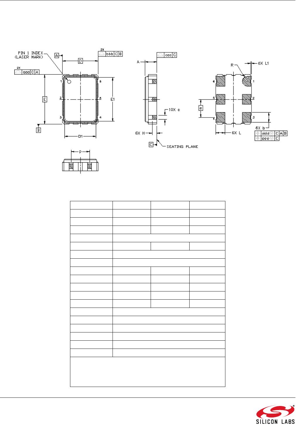
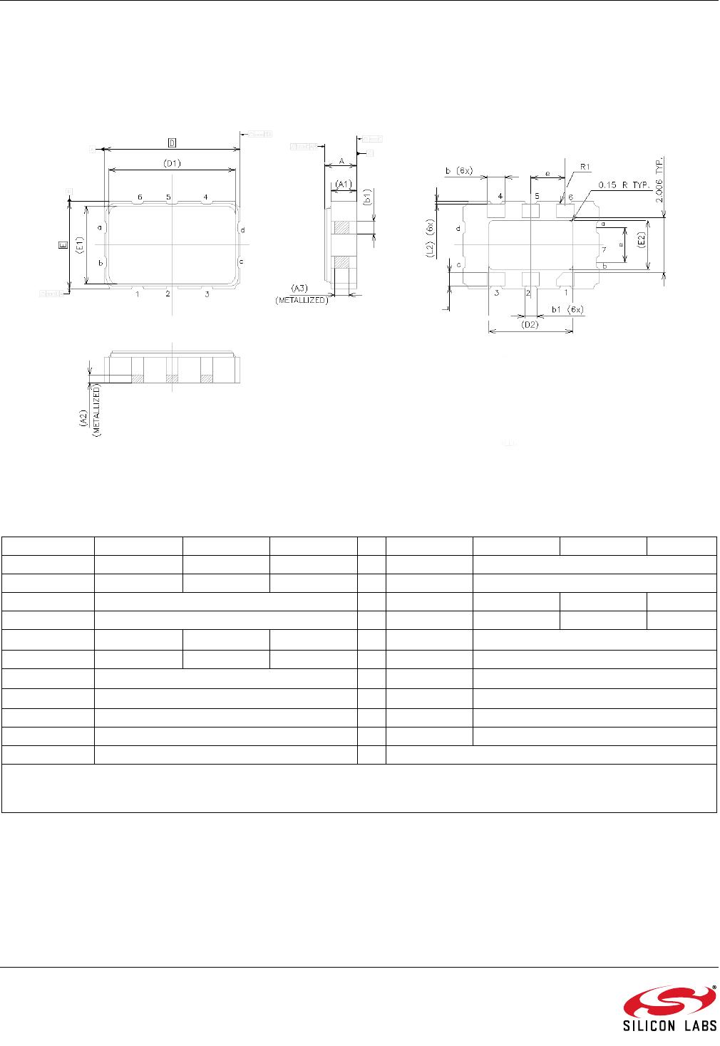
Si595
10 Rev. 1.4
4. Package Outline Diagram: 5x7mm, 6-pin
Figure 2 illustrates the package details for the 5 x 7 mm Si595. Table 12 lists the values for the dimensions shown
in the illustration.
Figure 2. Si595 Outline Diagram
Table 12. Package Diagram Dimensions (mm)
Dimension Min Nom Max
A 1.50 1.65 1.80
b 1.30 1.40 1.50
c 0.50 0.60 0.70
D 5.00 BSC
D1 4.30 4.40 4.50
e 2.54 BSC.
E 7.00 BSC.
E1 6.10 6.20 6.30
H 0.55 0.65 0.75
L 1.17 1.27 1.37
L1 0.05 0.10 0.15
p 1.80 2.60
R 0.70 REF
aaa 0.15
bbb 0.15
ccc 0.10
ddd 0.10
eee 0.05
Note:
1. All dimensions shown are in millimeters (mm) unless
otherwise noted.
2. Dimensioning and Tolerancing per ANSI Y14.5M-1994
Si595
Rev. 1.4 11
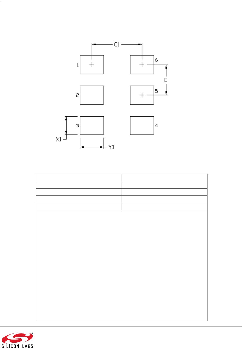
5. PCB Land Pattern: 5 x 7 mm, 6-pin
Figure 3 illustrates the 6-pin PCB land pattern for the 5 x 7 mm Si595. Table 13 lists the values for the dimensions
shown in the illustration.
Figure 3. Si595 PCB Land Pattern
Table 13. PCB Land Pattern Dimensions (mm)
Dimension (mm)
C1 4.20
E2.54
X1 1.55
Y1 1.95
Notes:
General
1. All dimensions shown are in millimeters (mm) unless otherwise noted.
2. Dimensioning and Tolerancing is per the ANSI Y14.5M-1994 specification.
3. This Land Pattern Design is based on the IPC-7351 guidelines.
4. All dimensions shown are at Maximum Material Condition (MMC). Least Material
Condition (LMC) is calculated based on a Fabrication Allowance of 0.05 mm.
Solder Mask Design
1. All metal pads are to be non-solder mask defined (NSMD). Clearance between
the solder mask and the metal pad is to be 60 µm minimum, all the way around
the pad.
Stencil Design
1. A stainless steel, laser-cut and electro-polished stencil with trapezoidal walls
should be used to assure good solder paste release.
2. The stencil thickness should be 0.125 mm (5 mils).
3. The ratio of stencil aperture to land pad size should be 1:1.
Card Assembly
1. A No-Clean, Type-3 solder paste is recommended.
2. The recommended card reflow profile is per the JEDEC/IPC J-STD-020
specification for Small Body Components.
Si595
12 Rev. 1.4
6. Package Outline Drawing: 3.2 x 5 mm, 6-pin
Figure 4 illustrates the package details for the 3.2 x 5 mm Si595. Table 14 lists the values for the dimensions
shown in the illustration.
Figure 4. Si595 Outline Diagram
Table 14. Package Diagram Dimensions (mm)
Dimension Min Nom Max Dimension Min Nom Max
A 1.02 1.17 1.32 E1 2.85 BSC
A1 0.99 1.10 1.21 E2 1.91 BSC
A2 0.5 BSC L 0.35 0.45 0.55
A3 0.30 BSC L2 0.05 0.10 0.15
b0.54
0.64 0.74
R1 0.10 REF
B1 0.35 0.45 0.55 aaa 0.15
D 5.00 BSC bbb 0.15
D1 4.65 BSC ccc 0.08
D2 3.38 BSC ddd 0.10
e 1.27 BSC eee 0.05
E 3.20 BSC
Notes:
1. All dimensions shown are in millimeters (mm) unless otherwise noted.
2. Dimensioning and Tolerancing per ANSI Y14.5M-1994.

595ND70M6560DGR

Mfr. #:
Manufacturer:
Silicon Labs
Description:
VCXO Oscillators Differential/single-ended single frequency VCXO; 10-810 MHz
Lifecycle:
New from this manufacturer.
Delivery:
DHL FedEx Ups TNT EMS
Payment:
T/T Paypal Visa MoneyGram Western Union