Si595
4 Rev. 1.4
Table 3. CLK± Output Frequency Characteristics
Parameter Symbol Test Condition Min Typ Max Units
Nominal Frequency
1,2,3
f
O
LVDS/CML/LVPECL 10 810
MHz
CMOS 10 160
Temperature Stability
1,4
T
A
= –40 to +85 ºC –20
–50
+20
+50
ppm
Absolute Pull Range
1,4
APR ±10 ±370 ppm
Power up Time
5
t
OSC
——10ms
Notes:
1. See Section 3. "Ordering Information" on page 9 for further details.
2. Specified at time of order by part number.
3. Nominal output frequency set by V
CNOM
=V
DD
/2.
4. Selectable parameter specified by part number.
5. Time from power up or tristate mode to f
O
.
Table 4. CLK± Output Levels and Symmetry
Parameter Symbol Test Condition Min Typ Max Units
LVPECL Output Option
1
V
O
mid-level V
DD
– 1.42 V
DD
– 1.25 V
V
OD
swing (diff) 1.1
1.9 V
PP
V
SE
swing (single-ended) 0.55
0.95 V
PP
LVDS Output Option
2
V
O
mid-level
1.125 1.20 1.275 V
V
OD
swing (diff)
0.5 0.7 0.9 V
PP
CML Output Option
2
V
O
2.5/3.3 V option mid-level V
DD
– 1.30
V
1.8 V option mid-level V
DD
– 0.36
V
OD
2.5/3.3 V option swing (diff) 1.10 1.50 1.90
V
PP
1.8 V option swing (diff) 0.35 0.425 0.50
CMOS Output Option
3
V
OH
0.8 x V
DD
V
DD
V
V
OL
——0.4
Rise/Fall time (20/80%)
t
R,
t
F
LVPECL/LVDS/CML 350 ps
CMOS with C
L
=15pF 2 ns
Symmetry (duty cycle) SYM LVPECL: V
DD
– 1.3 V (diff)
LVDS: 1.25 V (diff)
CMOS: V
DD
/2
45 55 %
Notes:
1. 50 to V
DD
– 2.0 V.
2. R
term
= 100 (differential).
3. C
L
= 15 pF. Sinking or sourcing 12 mA for V
DD
= 3.3V, 6mA for V
DD
= 2.5V, 3mA for V
DD
= 1.8 V.
Si595
Rev. 1.4 5
Table 5. CLK± Output Phase Jitter
Parameter Symbol Test Condition Min Typ Max Units
Phase Jitter (RMS)
1,2
for F
OUT
of 50 MHz < F
OUT
810 MHz
J
Kv = 45 ppm/V
12 kHz to 20 MHz 0.5
ps
Kv = 95 ppm/V
12 kHz to 20 MHz 0.5
Kv = 125 ppm/V
12 kHz to 20 MHz 0.5
Kv = 185 ppm/V
12 kHz to 20 MHz 0.5
Kv = 380 ppm/V
12 kHz to 20 MHz 0.7
Notes:
1. Refer to AN256 for further information.
2. For best jitter and phase noise performance, always choose the smallest K
V
that meets the application’s minimum APR
requirements. See “AN266: VCXO Tuning Slope (K
V
), Stability, and Absolute Pull Range (APR)” for more information.
Table 6. CLK± Output Period Jitter
Parameter Symbol Test Condition Min Typ Max Units
Period Jitter* J
PER
RMS 3 ps
Peak-to-Peak 35
*Note: Any output mode, including CMOS, LVPECL, LVDS, CML. N = 1000 cycles. Refer to AN279 for further information.
Table 7. CLK± Output Phase Noise (Typical)
Offset Frequency 74.25 MHz
185 ppm/V
LVPECL
148.5 MHz
185 ppm/V
LVPECL
155.52 MHz
95 ppm/V
LVPECL
Units
100 Hz
1kHz
10 kHz
100 kHz
1MHz
10 MHz
20 MHz
–77
–101
–121
–134
–149
–151
–150
–68
–95
–116
–128
–144
–147
–148
–77
–101
–119
–127
–144
–147
–148
dBc/Hz
Si595
6 Rev. 1.4
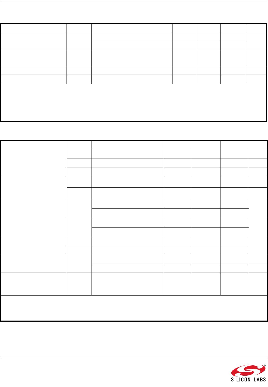
Table 8. Environmental Compliance and Package Information
Parameter Conditions/Test Method
Mechanical Shock MIL-STD-883, Method 2002
Mechanical Vibration MIL-STD-883, Method 2007
Solderability MIL-STD-883, Method 2003
Gross and Fine Leak MIL-STD-883, Method 1014
Resistance to Solder Heat MIL-STD-883, Method 2036
Contact Pads Gold over Nickel
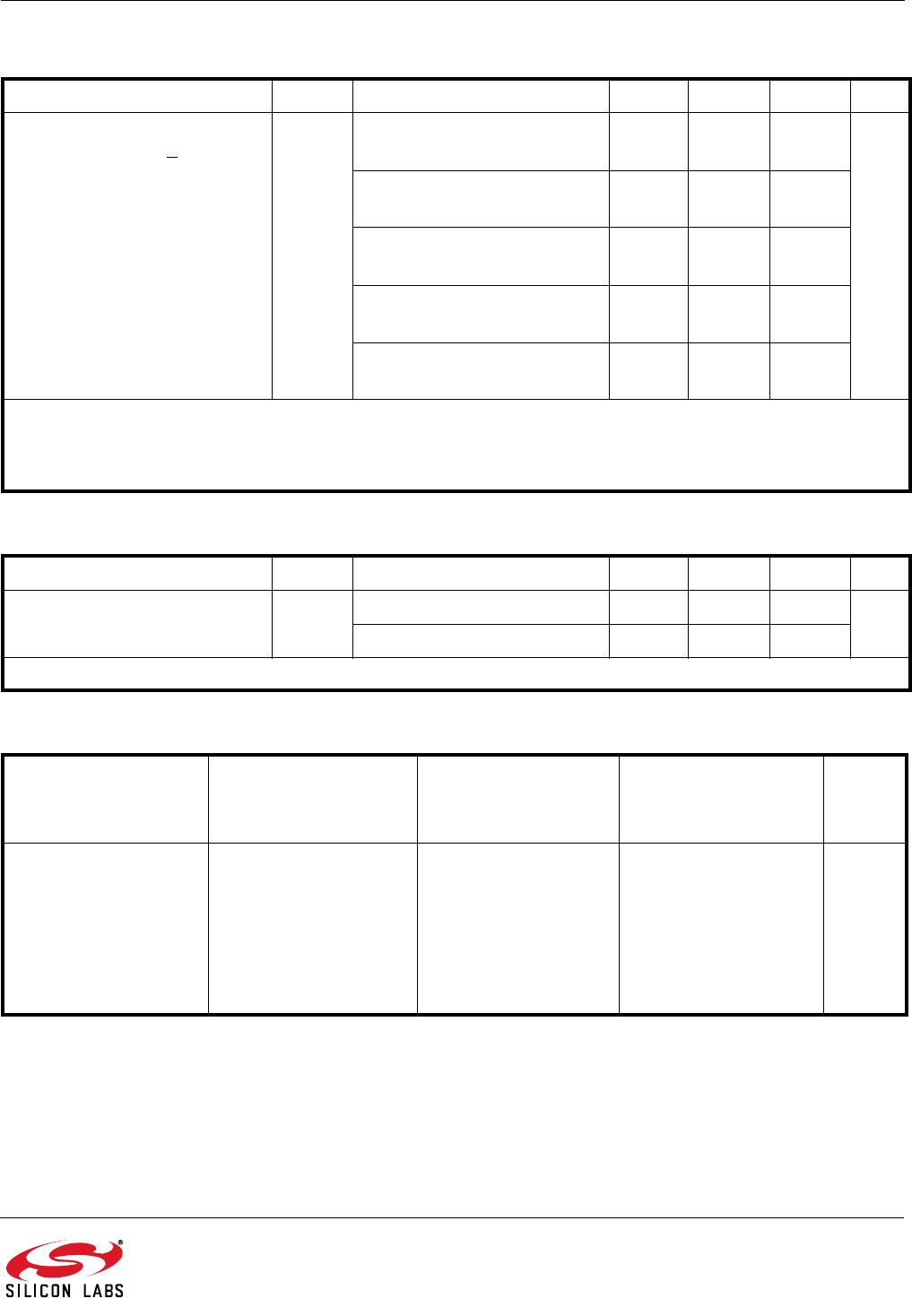
Table 9. Thermal Characteristics
(Typical values TA = 25 ºC, V
DD
=3.3V)
Parameter Symbol Test Condition Min Typ Max Unit
5x7mm, Thermal Resistance Junction to
Ambient
JA
Still Air 84.6 °C/W
5x7mm, Thermal Resistance Junction to
Case
JC
Still Air 38.8 °C/W
3.2x5mm, Thermal Resistance Junction to
Ambient
JA
Still Air 31.1 °C/W
3.2x5mm, Thermal Resistance Junction to
Case
JC
Still Air 13.3 °C/W
Ambient Temperature T
A
–40 85 °C
Junction Temperature T
J
——125°C
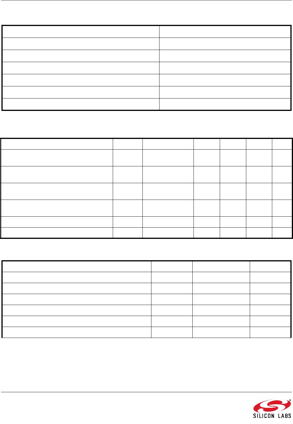
Table 10. Absolute Maximum Ratings
1
Parameter Symbol Rating Units
Maximum Operating Temperature T
AMAX
85 ºC
Supply Voltage V
DD
–0.5 to +3.8 V
Input Voltage V
I
–0.5 to V
DD
+ 0.3
Storage Temperature T
S
–55 to +125 ºC
ESD Sensitivity (HBM, per JESD22-A114) ESD 2500 V
Soldering Temperature (Pb-free profile)
2
T
PEAK
260 ºC

595ND70M6560DGR

Mfr. #:
Manufacturer:
Silicon Labs
Description:
VCXO Oscillators Differential/single-ended single frequency VCXO; 10-810 MHz
Lifecycle:
New from this manufacturer.
Delivery:
DHL FedEx Ups TNT EMS
Payment:
T/T Paypal Visa MoneyGram Western Union