Rev. 1.4 9
3. Ordering Information
. Specific device configurations are programmed into the Si595 at time of shipment. Configurations are
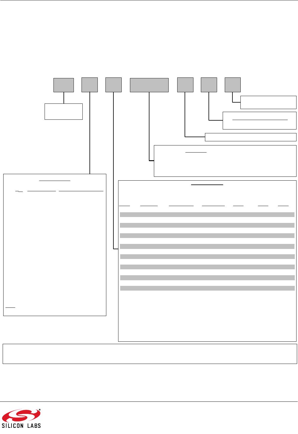
Figure 1. Part Number Convention
R = Tape and Reel
Blank = Coil Tape
Operating Temp Range (°C)
G –40 to +85 °C
Device Revision Letter
595 VCXO
Product Family
595 X X XXXMXXX D G R
1
st
Option Code
V
DD
Output Format Output Enable Polarity
A 3.3 LVPECL High
B 3.3 LVDS High
C3.3CMOS High
D3.3CML High
E 2.5 LVPECL High
F 2.5 LVDS High
G2.5CMOS High
H2.5CML High
J 1.8 CMOS High
K1.8CML High
M 3.3 LVPECL Low
N 3.3 LVDS Low
P 3.3 CMOS Low
Q 3.3 CML Low
R 2.5 LVPECL Low
S 2.5 LVDS Low
T 2.5 CMOS Low
U 2.5 CML Low
V 1.8 CMOS Low
W 1.8 CML Low
Note:
CMOS available to 160 MHz.
2
nd
Option Code
Temperature Tuning Slope Minimum APR
Stability Kv (±ppm) for VDD @
Code Package ± ppm (max) ppm/V (typ) 3.3 V 2.5 V 1.8 V
A 5x7 mm 20 380 370 275 200
B 5x7 mm 20 185 160 110 80
C 5x7 mm 50 185 130 80 50
D 5x7 mm 20 125 100 75 40
E 5x7 mm 20 95 65 50 25
F 5x7 mm 50 125 70 45 10
G 5x7 mm 50 95 35 20 N/A
H 5x7 mm 20 45 15 N/A N/A
J 3.2x5 mm 20 380 370 275 200
K 3.2x5 mm 20 185 160 110 80
M 3.2x5 mm 50 185 130 80 50
P 3.2x5 mm 20 125 100 75 40
Q 3.2x5 mm 20 95 65 50 25
R 3.2x5 mm 50 125 70 45 10
S 3.2x5 mm 50 95 35 20 N/A
T 3.2x5 mm 20 45 15 N/A N/A
Notes:
1. For best jitter and phase noise performance, always choose the smallest Kv that meets
the application’s minimum APR requirements. Lower Kv options minimize noise
coupling and jitter in real-world PLL designs. See AN266 for more information.
2. APR is the ability of a VCXO to track a signal over the product lifetime. A VCXO with an
APR of ±100 ppm is able to lock to a clock with a ±100 ppm stability over 15 years over
all operating conditions.
3. Nominal Pull range (±) = 0.5 x V
DD
x tuning slope.
4. Minimum APR values noted above include worst case values for all parameters.
Example Part Number: 595AE148M500DGR is a 5 x 7 mm VCXO in a 6 pad package. The nominal frequency is 148.5 MHz, with a 3.3 V supply,
LVPECL output, and Output Enable active high polarity. Temperature stability is specified as ±20 ppm and the tuning slope is 95 ppm/V. The part is
specified for a –40 to +85 C° ambient temperature range operation and is shipped in tape and reel format.
Frequency(e.g., 148M500 is 148.5 MHz)
Available frequency range is 10 to 810 MHz. The position of “M” shifts
to denote higher or lower frequencies. If the frequency of interest
requires greater than 6 digit resolution, a six digit code will be
assigned for the specific frequency.