© Semiconductor Components Industries, LLC, 2014
December, 2014 − Rev. 6
1 Publication Order Number:
NCP308/D
NCP308, NCV308
Low Quiescent Current,
Programmable Delay Time,
Supervisory Circuit
The NCP308 series is one of the ON Semiconductor Supervisory
circuit IC families. It is optimized to monitor system voltages from
0.405 V to 5.5 V, asserting an active low open−drain RESET
output,
together with Manual Reset (MR
) Input. The part comes with both
fixed and externally adjustable versions.
Features
• Wide Supply Voltage Range 1.6 to 5.5 V
• Very Low Quiescent Current 1.6 mA
• Fixed Threshold Voltage Versions for Standard Voltage Rails
Including 0.9 V, 1.2 V, 1.25 V, 1.5 V, 1.8 V, 1.9 V, 2.5 V, 2.8 V, 3.0 V,
3.3 V, 5.0 V
• Adjustable Version with Low Threshold Voltage 0.405 V (min)
• High Threshold Voltage Accuracy: 0.31% typ
• Support Manual Reset Input ( MR)
• Open−Drain RESET Output (Push−pull Output upon Request)
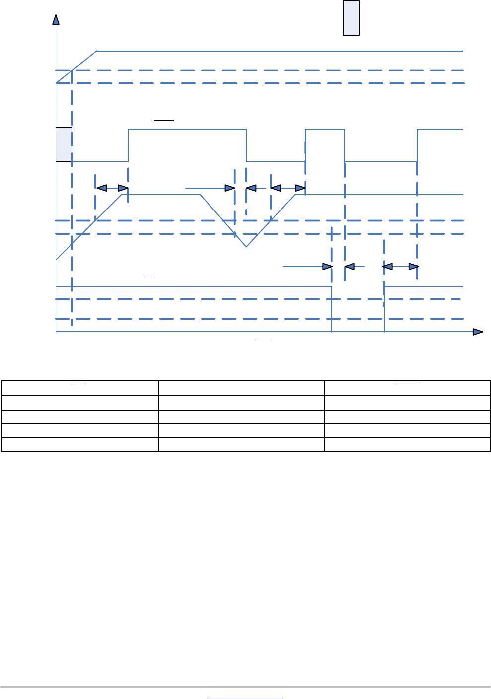
• Flexible Delay Time Programmability: 1.25 ms to 10 s
• Temperature Range: −40°C to +125°C
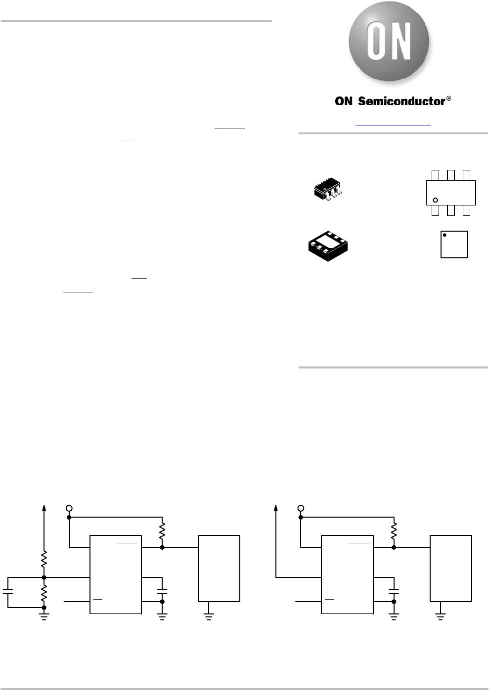
• Small TSOP−6 and WDFN6 2 x 2 mm, Pb−Free packages
• NCV Prefix for Automotive and Other Applications Requiring
Unique Site and Control Change Requirements; AEC−Q100
Qualified and PPAP Capable
• These are Pb−Free Devices
Typical Applications
• DSP or Microcontroller Applications
• Notebook/Desktop Computers
• PDAs/Hand−Held Products
• Portable/Battery−Powered Products
• FPGA/ASIC Applications
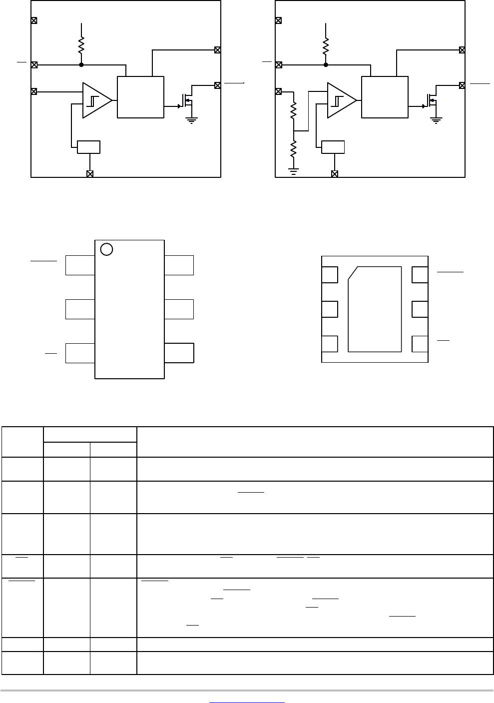
MR
VDD
(Optional)
Rpullup
SENSE CT
GND
VDD
CT
R1
R2
Figure 1. Typical Application Circuit for Adjustable
Versions
1 nF
(Optional)
NCP308XXADJ
DSP/
RESET
Figure 2. Typical Application Circuit for Fixed
Versions
Processor
VIN
MR
RESET
MR
VDD
(Optional)
Rpullup
SENSE CT
GND
VDD
CT
DSP/
RESET
Processor
VIN
MR
RESET
See detailed ordering and shipping information in the ordering
information section on page 9 of this data sheet.
ORDERING INFORMATION
TSOP−6
CASE 318G
www.onsemi.com
MARKING
DIAGRAMS
(Note: Microdot may be in either location)
1
XXX, XX= Specific Device Code
A =Assembly Location
Y = Year
W = Work Week
M = Date Code
G = Pb−Free Package
XXXAYWG
G
1
WDFN6
CASE 511BR
XX M
1