NCP308MT120TBG

NCP308, NCV308
www.onsemi.com
7
DETAILED DESCRIPTION
The NCP308 microprocessor supervisory product family
is designed to assert a RESET
signal when either the SENSE
pin voltage drops below V
IT
or the Manual Reset input (MR)
is driven low. The RESET
output remains asserted for a
programmable delay time after both MR
and SENSE
voltages return above the respective thresholds. A broad
range of voltage threshold and reset delay time options are
available, allowing NCP308 series to be used in a wide range
of applications.
Reset threshold voltages can be factory−set from 0.82 V
to 3.3 V or from 4.4 V to 5.0 V, while the NCP308XXADJ
can be used for any voltage above 0.405 V using an external
resistor divider.
Flexible delay time can be easily got with CT pin
according to Table 5:
Table 5. DELAY TIME SETTING TABLE
CT pin Configuration Delay Time (tD)
CT = VDD 300 ms (fixed)
CT = Open 20 ms (fixed)
Connecting a capacitor be-
tween pin CT and GND
(Capacitor CT value >
100 pF)
1.25 ms ~ 10 s, depends on
capacitor value (Refer to the
Setting Reset Delay Time
Section)
Output
The RESET output is typically connected to the RESET
control pin of a microprocessor. For Open−Drain output
versions, a pull−up resistor must be used to hold this line
high when RESET
is not asserted. The RESET output is
active once V
DD
is over V
DD
(min), this voltage is much
lower than most microprocessors’ functional voltage range.
RESET
remains high as long as SENSE is above its
threshold (V
IT
) and the Manual Reset input (MR) is logic
high. If either SENSE falls below V
IT
or MR is driven low,
RESET
is asserted.
Once MR
is again logic high and SENSE is above (V
IT
+
V
HYS
), the RESET pin goes to a high impedance state after
delay time (tD). The open−drain structure of RESET
is
capable to allow the reset signal for the microprocessor to
have a voltage higher than V
DD
(up to 5.5 V). The pull−up
resistor should be no smaller than 10 kW as a result of the
finite impedance of the RESET
line.
SENSE Input
The SENSE input should be connected to the monitored
voltage directly. If the voltage on this pin drops below V
IT
,
then RESET
is asserted. The comparator has a built−in
hysteresis to prevent erratic reset operation. It is good
practice to put a 1 nF to 10 nF bypass capacitor on the
SENSE input to reduce its sensitivity to transients and layout
parasitic.
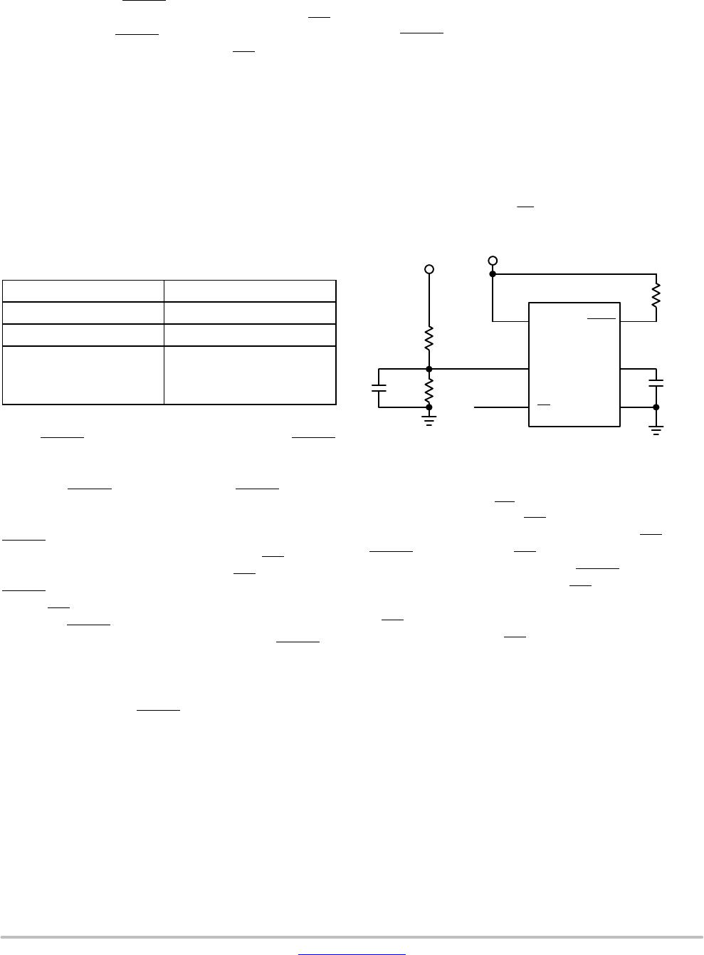
The NCP308XXADJ can be used to monitor any voltage
rail down to 0.405 V by the circuit shown in Figure 12. The
new V
IT
’ can be derived from resistor divider network of R1
and R2 by:
V
IT
Ȁ+
ǒ
R1
R2
) 1
Ǔ
V
IT
(eq. 1)
VIN
VDD
(Optional)
Rpullup
SENSE CT
GND
VDD
CT
R1
R2
1 nF
(Optional)
NCP308XXADJ
Figure 12. Using NCP308XXADJ to Monitor a
User−Defined Threshold Voltage
MR
RESET
MR
Manual Reset Input (MR)
The Manual Reset input (MR) allows a processor or other
logic circuits to initiate a reset. A logic low on MR
causes
RESET
to assert. After MR returns to a logic high and
SENSE is above its reset threshold, RESET
is de−asserted
after the delay time set by CT pin. MR
is internally tied to
V
DD
by a 90 kW resistor so this pin can be left unconnected
if MR
will not be used.
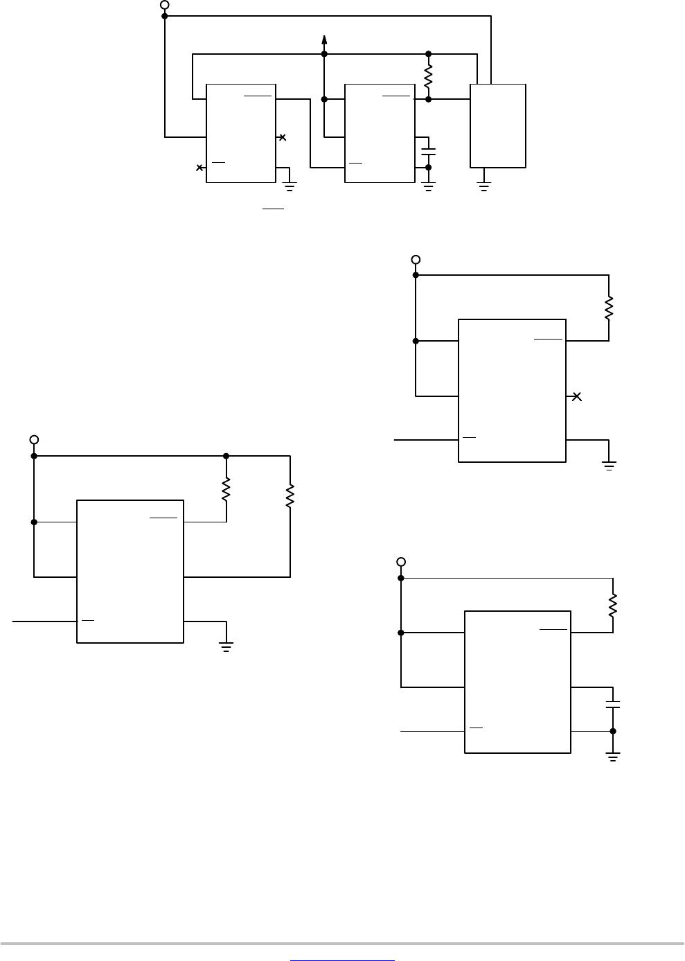
Figure 13 shows how MR
can be used to monitor multiple
system voltages (e.g. I/O supply voltage of some
DSP/processors should be setup before core voltage, and
DSP/processor can only start after both I/O and core
voltages setup).
NCP308, NCV308
www.onsemi.com
8
NCP308XX330
SENSE
CT
GND
VDD
NCP308XX120
SENSE CT
GND
VDD
3.3 V
DSP/
RESET
VIO
1.2 V
Vcore
Figure 13. Using MR to Monitor Multiple System Voltages
MR
RESET
Processor
MR
RESET
Setting Reset Delay Time
The NCP308 has three options for setting the reset delay
time as shown in Table 5. Figure 14 shows the configuration
for a fixed 300 ms typical delay time by tying CT to V
DD
;
a resistor from 40 kW to 200 kW must be used. Figure 15
shows a fixed 20 ms delay time by leaving the CT pin
unconnected.
Figure 16 shows a user−defined program time between
1.25 ms and 10 s by connecting a capacitor between CT pin
and ground.
3.3 V
MR
Rpullup
SENSE CT
GND
VDD
50k
Figure 14. Delay Time Fixed to 300 ms when CT
Connected to VDD by Resistor
MR
RESET
3.3V
MR
Rpullup
SENSE CT
GND
VDD
Figure 15. Delay Time Fixed to 20 ms when CT is
Open
MR
RESET
3.3 V
MR
Rpullup
SENSE CT
GND
VDD
CT
Figure 16. Delay Time Set by Capacitor
MR
RESET
The capacitor CT should be 100 pF for NCP308 to
recognize that the capacitor is present. The capacitor value
for a given delay time can be calculated using the following
equation:
NCP308, NCV308
www.onsemi.com
9
CT(nF) +
ǒ
tD(s) * 0.5 10
−3
(s)
Ǔ
175
(eq. 2)
Parasitic capacitances of CT pin should be considered to
avoid reset delay time deviation or error.
Immunity to Sense Pin Voltage Transients
NCP308 is relatively immune to short negative transients
on SENSE pin. Sensitivity to transients is dependent on
threshold overdrive, as shown in the Maximum Transient
Duration at Sense vs. Sense Threshold Overdrive Voltage
graph (Figure 9) in Typical Operating Characteristics
section.
ORDERING INFORMATION
Device Status (Note 6)
Threshold
Voltage
(V
IT
)
Nominal
Monitored
Voltage
Marking Package Shipping
NCP308SNADJT1G Active 0.405 V
Adjustable
Version
ADJ
TSOP−6
(Pb−Free)
3000 / Tape & Reel
NCV308SNADJT1G* Active 0.405 V VDJ
NCP308SN090T1G Active 0.84 V 0.9 V 090
NCP308SN120T1G Active 1.12 V 1.2 V 120
NCP308SN125T1G Active 1.16 V 1.25 V 125
NCP308SN150T1G Active 1.40 V 1.5 V 150
NCP308SN180T1G Active 1.67 V 1.8 V 180
NCP308SN190T1G Active 1.77 V 1.9 V 190
NCP308SN250T1G Active 2.33 V 2.5 V 250
NCP308SN280T1G Active 2.61 V 2.8 V 280
NCP308SN300T1G Active 2.79 V 3.0 V 300
NCP308SN330T1G Active 3.07 V 3.3 V 330
NCV308SN330T1G* Active 3.07 V 3.3 V 33A
NCP308SN500T1G Active 4.65 V 5.0 V 500
NCP308MTADJTBG Active 0.405 V Adjustable
Version
AA
WDFN6
(Pb−Free)
NCP308MT090TBG Active 0.84 V 0.9 V AC
NCP308MT120TBG Active 1.12 V 1.2 V AD
NCP308MT125TBG Active 1.16 V 1.25 V AE
NCP308MT150TBG Active 1.40 V 1.5 V AF
NCP308MT180TBG Active 1.67 V 1.8 V AG
NCP308MT190TBG Active 1.77 V 1.9 V AH
NCP308MT250TBG Active 2.33 V 2.5 V AJ
NCP308MT280TBG Active 2.61 V 2.8 V AK
NCP308MT300TBG Active 2.79 V 3.0 V AL
NCP308MT330TBG Active 3.07 V 3.3 V AM
NCP308MT500TBG Active 4.65 V 5.0 V AN
For information on tape and reel specifications, including part orientation and tape sizes, please refer to our Tape and Reel Packaging
Specifications Brochure, BRD8011/D.
*NCV Prefix for Automotive and Other Applications Requiring Unique Site and Control Change Requirements; AEC−Q100 Qualified and PPAP
Capable.
6. The marketing status are defined as below:
Active: Products in production and recommended for new designs;
Under Request: Device has been announced but is not in production. Samples may or may not be available.

NCP308MT120TBG

Mfr. #:
Manufacturer:
ON Semiconductor
Description:
Supervisory Circuits 1.2V NCP308 WDFN6
Lifecycle:
New from this manufacturer.
Delivery:
DHL FedEx Ups TNT EMS
Payment:
T/T Paypal Visa MoneyGram Western Union