NCP308, NCV308
www.onsemi.com
4
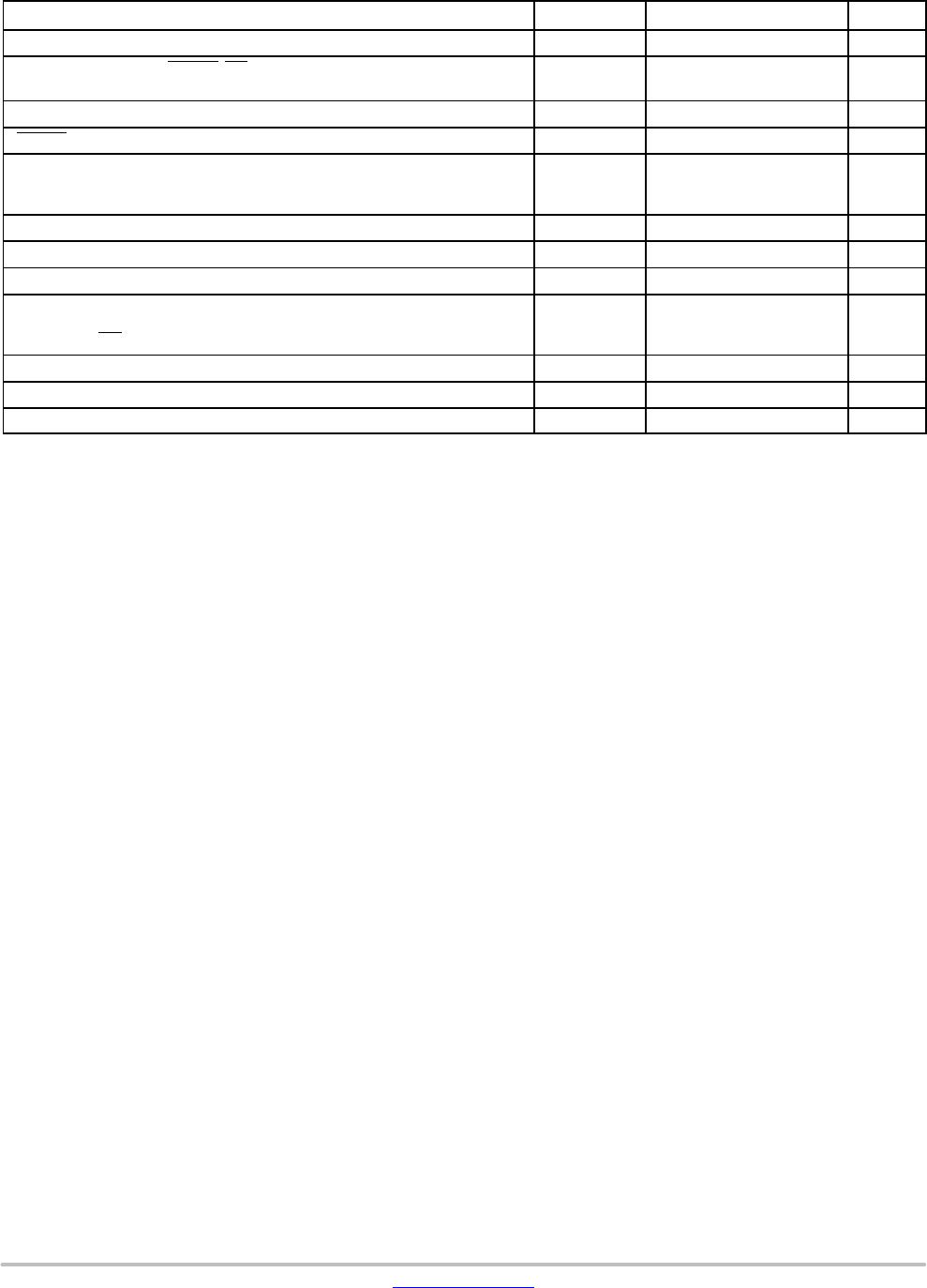
Table 3. MAXIMUM RATINGS
Rating Symbol Value Unit
Input voltage range, V
DD
V
DD
−0.3 to + 6.0 V
CT voltage range V
CT
, RESET, MR
Current through CT pin
I
CT
−0.3 to V
DD
+0.3 ≤ 6.0
10
V
mA
SENSE pin voltage −0.3 to + 8.0 V
RESET pin current 5 mA
Thermal Resistance Junction−to−Air
TSOP−6
WDFN6
R
q
JA
305
220
°C/W
Human Body Model (HBM) ESD Rating (Note 1) ESD HBM 2000 V
Machine Model (MM) ESD Rating (Note 1) ESD MM 100 V
Charged Device Model (CDM) ESD Rating (Note 1) ESD CDM 500 V
Latch up Current: (Note 2)
All pins, except digital pins
Digital pins (MR)
I
LU
±100
±10
mA
Storage Temperature Range T
STG
−65 to + 150 °C
Maximum Junction Temperature T
J
−40 to +150 °C
Moisture Sensitivity (Note 3) MSL Level 1
Stresses exceeding those listed in the Maximum Ratings table may damage the device. If any of these limits are exceeded, device functionality
should not be assumed, damage may occur and reliability may be affected.
1. This device series contains ESD protection and passes the following tests:
Human Body Model (HBM) +/−2.0 kV per JEDEC standard: JESD22−A114
Machine Model (MM) +/−100 V per JEDEC standard: JESD22−A115
Charged Device Model (CDM) 500 V per JEDEC standard: JESD22−C101.
2. Latch up Current per JEDEC standard: JESD78 class II.
3. Moisture Sensitivity Level (MSL): 1 per IPC/JEDEC standard: J−STD−020A.

