ADuM4120/ADuM4120-1 Data Sheet
Rev. 0 | Page 10 of 17
0
0.5
1.0
1.5
2.0
2.5
3.0
3.5
4.0
4.5
5.0
0 20406080100
I
DD2
(mA)
DUTY CYCLE (%)
V
DD2
= 15V
V
DD2
= 5V
V
DD2
= 10V
15493-010
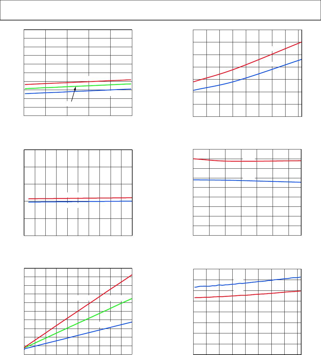
Figure 10. I
DD2
vs. Duty Cycle, V
DD1
= 5 V, f
SW
= 10 kHz, 2 nF Load
0
1
2
3
4
5
0 50 100 150 200 250 300 350 400 450 500
I
DD1
(mA)
SWITCHING FREQUENCY (kHz)
V
DD1
= 5V
V
DD1
= 3.3V
15493-011
Figure 11. I
DD1
vs. Switching Frequency
0
2
4
6
8
10
12
14
16
18
20
0 50 100 150 200 250 300 350 400 450 500
I
DD2
(mA)
FREQUENCY (kHz)
V
DD2
= 15V
V
DD2
= 5V
V
DD2
= 10V
15493-012
Figure 12. I
DD2
vs. Switching Frequency, 2 nF Load
0
0.2
0.4
0.6
0.8
1.0
1.2
1.4
–40 –20 0 20 40 60 80 100 120
TEMPERATUREC)
R
DSON_x
()
NMOS
PMOS
15493-013
Figure 13. R
DSON_x
vs. Temperature
0
0.1
0.2
0.3
0.4
0.5
0.6
0.7
0.8
0.9
4.5 9.0 13.5 18.0 22.5 27.0 31.5
V
DD2
(V)
R
DSON_x
()
PMOS
NMOS
15493-014
Figure 14. R
DSON_x
vs. V
DD2
0
10
20
30
40
50
60
70
80
–40 –20 0 20 40 60 80 100 120
PROPAGATION DELAY (ns)
TEMPERATURE (°C)
t
DHL
t
DLH
15493-015
Figure 15. ADuM4120 Propagation Delay vs. Temperature, 2 nF Load
Data Sheet ADuM4120/ADuM4120-1
Rev. 0 | Page 11 of 17
0
10
20
30
40
50
60
70
80
–40 –20 0 20 40 60 80 100 120
PROPAGATION DELAY (ns)
TEMPERATURE (ºC)
15493-016
t
DHL
t
DLH
Figure 16. ADuM4120-1 Propagation Delay vs. Temperature, 2 nF Load
0
10
20
30
40
50
60
70
80
90
100
4.5 9.5 14.5 19.5 24.5 29.5 34.5
PROPA
G
A
TION DEL
A
Y (ns)
V
DD2
(V)
15493-017
t
DHL
t
DLH
Figure 17. ADuM4120 Propagation Delay vs. V
DD2
, 2 nF Load
0
10
20
30
40
50
60
70
80
90
100
4.5 9.5 14.5 19.5 24.5 29.5 34.5
PROPAGATION DELAY (ns)
V
DD2
(V)
15493-018
t
DHL
t
DLH
Figure 18. ADuM4120-1 Propagation Delay vs. V
DD2
, 2 nF Load
0
1
2
3
4
5
6
7
8
9
10
4.5 9.5 14.5 19.5 24.5 29.5 34.5
PEAK CURRENT (A)
V
DD2
(V)
SOURCE CURRENT
SINK CURRENT
15493-019
Figure 19. Peak Current vs. V
DD2
, 2 Ω Resistor
Data Sheet ADuM4120/ADuM4120-1
Rev. 0 | Page 12 of 17
THEORY OF OPERATION
Gate drivers are required in situations where fast rise times of
switching device gates are desired. The gate signal for most
enhancement type power devices are referenced to a source or
emitter node. The gate driver must be able to follow this source
or emitter node, necessitating isolation between the controlling
signal and the output of the gate driver in topologies where the
source or emitter nodes swing, such as a half bridge. Gate switching
times are a function of the drive strength of the gate driver. Buffer
stages before a CMOS output reduce total delay time and
increase the final drive strength of the driver.
The ADuM4120/ADuM4120-1 achieve isolation between the
control side and the output side of the gate driver by means of
a high frequency carrier that transmits data across the isolation
barrier using iCoupler chip scale transformer coils separated by
layers of polyimide isolation. The encoding scheme used by the
ADuM4120/ADuM4120-1 is a positive logic on/off keying (OOK),
meaning a high signal is transmitted by the presence of the carrier
frequency across the iCoupler chip scale transformer coils. Positive
logic encoding ensures that a low signal is seen on the output
when the input side of the gate driver is not powered. A low state is
the most common safe state in enhancement mode power devices,
driving in situations where shoot through conditions can exist.
The architecture is designed for high common-mode transient
immunity and high immunity to electrical noise and magnetic
interference. Radiated emissions are minimized with a spread
spectrum OOK carrier and other techniques such as differential
coil layout. Figure 20 illustrates the encoding used by the
ADuM4120/ADuM4120-1.
TRANSMITTER
GND
1
GND
2
V
IN
V
OUT
RECEIVER
REGULATOR REGULATOR
15493-120
Figure 20. Operational Block Diagram of OOK Encoding
ADUM4120-1ARIZ

Mfr. #:
Manufacturer:
Analog Devices Inc.
Description:
Gate Drivers Iso Gate Drvr w/2A output
Lifecycle:
New from this manufacturer.
Delivery:
DHL FedEx Ups TNT EMS
Payment:
T/T Paypal Visa MoneyGram Western Union