ADuM4120/ADuM4120-1 Data Sheet
Rev. 0 | Page 4 of 17
Parameter Symbol Min Typ Max Unit Test Conditions/Comments
SWITCHING SPECIFICATIONS
Pulse Width PW 50 ns C
L
= 2 nF, V
DD2
= 15 V, R
GON
= R
GOFF
= 5 Ω
Deglitch (V
IN
) t
IN_IN
, t
IN_NIN
20 ns
ADuM4120
Propagation Delay
1
C
L
= 2 nF, V
DD2
= 15 V, R
GON
= R
GOFF
= 5 Ω
Rising Edge t
DLH
44 57 68 ns
Falling Edge t
DHL
55 66 79 ns
Skew t
PSK
25 ns C
L
= 2 nF, R
GON
= R
GOFF
= 5 Ω
Rising Edge t
PSKLH
19 ns
Falling Edge t
PSKHL
13 ns
Pulse Width Distortion t
PWD
9 16.5 ns C
L
= 2 nF, V
DD2
= 15 V, R
GON
= R
GOFF
= 5 Ω
ADuM4120-1
Propagation Delay
1
C
L
= 2 nF, V
DD2
= 15 V, R
GON
= R
GOFF
= 5 Ω
Rising Edge t
DLH
22 33 42 ns
Falling Edge t
DHL
36 43 58 ns
Skew t
PSK
25 ns C
L
= 2 nF, R
GON
= R
GOFF
= 5 Ω
Rising Edge t
PSKLH
14 ns
Falling Edge t
PSKHL
12 ns
Pulse Width Distortion t
PWD
9 16.5 ns C
L
= 2 nF, V
DD2
= 15 V, R
GON
= R
GOFF
= 5 Ω
OUTPUT RISE/FALL TIME (10% TO 90%) t
R
/t
F
11 18 26 ns C
L
= 2 nF, V
DD2
= 15 V, R
GON
= R
GOFF
= 5 Ω
COMMON-MODE TRANSIENT IMMUNITY
(CMTI)
|CMTI|
Static CMTI
2
150 kVs V
CM
= 1500 V
Dynamic CMTI
3
150 kVs V
CM
= 1500 V
1
t
DLH
propagation delay is measured from the time of the input rising logic high voltage threshold, VIH, to the output rising 10% level of the V
OUT
signal. t
DHL
propagation
delay is measured from the input falling logic low voltage threshold, VIL, to the output falling 90% threshold of the V
OUT
signal. See Figure 22 for waveforms of propagation delay
parameters.
2
Static CMTI is the largest dv/dt between GND
1
and GND
2
, with inputs held either high or low, such that the output voltage remains either above 0.8 × V
DD2
for output high
or 0.8 V for output low. Operation with transients above recommended levels can cause momentary data upsets.
3
Dynamic CMTI is the largest dv/dt between GND
1
and GND
2
with the switching edge coincident with the transient test pulse. Operation with transients above the
recommended levels can cause momentary data upsets.
REGULATORY INFORMATION
The ADuM4120/ADuM4120-1 are pending approval by the organizations listed in Table 2.
Table 2.
UL (Pending) CSA (Pending) VDE (Pending) CQC (Pending)
UL1577 Component
Recognition Program
Approved under CSA Component Acceptance
Notice 5A
DIN V VDE V 0884-10
(VDE V 0884-10):2006-12
Certified under CQC11-
471543-2012
Single Protection, 5000 V rms
Isolation Voltage
CSA 60950-1-07+A1+A2 and IEC 60950-1,
second edition, +A1+A2:
Reinforced insulation,
849 V peak, V
IOSM
= 10 kV peak
GB4943.1-2011
Basic insulation at 800 V rms (1131 V peak)
Basic insulation 849 V peak,
V
IOSM
= 16 kV peak
Basic insulation at 800 V rms
(1131 V peak)
Reinforced insulation at 400 V rms (565 V peak)
Reinforced insulation at
400 V rms (565 V peak)
IEC 60601-1 Edition 3.1:
Basic insulation (1 MOPP), 500 V rms (707 V peak)
Reinforced insulation (2 MOPP), 250 V rms
(1414 V peak)
CSA 61010-1-12 and IEC 61010-1 third edition
Basic insulation at: 600 V rms mains, 800 V
secondary (1089 V peak)
Reinforced insulation at: 300 V rms mains,
400 V secondary (565 V peak)
File E214100 File 205078 File 2471900-4880-0001 File (pending)
Data Sheet ADuM4120/ADuM4120-1
Rev. 0 | Page 5 of 17
PACKAGE CHARACTERISTICS
Table 3.
Parameter Symbol Min Typ Max Unit Test Conditions/Comments
Resistance (Input Side to High-Side Output)
1
R
I-O
10
12
Ω
Capacitance (Input Side to High-Side Output)
1
C
I-O
2.0 pF
Input Capacitance C
I
4.0 pF
Junction to Ambient Thermal Resistance θ
JA
123.7 °C/W
4-layer printed circuit
board (PCB)
1
The device is considered a 2-terminal device: Pin 1 through Pin 3 are shorted together, and Pin 4 through Pin 6 are shorted together.
INSULATION AND SAFETY RELATED SPECIFICATIONS
Table 4.
Parameter Symbol Value Unit Conditions
Rated Dielectric Insulation Voltage 5000 V rms 1 minute duration
Minimum External Air Gap (Clearance) L(I01) 8 min mm
Measured from input terminals to output terminals,
shortest distance through air
Minimum External Tracking (Creepage) L(I02) 8 min mm
Measured from input terminals to output terminals,
shortest distance path along body
Minimum Clearance in the Plane of the PCB Clearance
L(PCB) 8.3 min mm
Measured from input terminals to output terminals,
shortest distance through air, line of sight, in the PCB
mounting plane
Minimum Internal Gap (Internal Clearance) 25.5 min μm Insulation distance through insulation
Tracking Resistance (Comparative Tracking Index) CTI >400 V DIN IEC 112/VDE 0303 Part 3
Isolation Group II Material Group (DIN VDE 0110, 1/89, Table 1)
DIN V VDE V 0884-10 (VDE V 0884-10) INSULATION CHARACTERISTICS
This isolator is suitable for reinforced isolation only within the safety limit data. Maintenance of the safety data is ensured by protective circuits.
Table 5. VDE Characteristics
Description Test Conditions/Comments Symbol Characteristic Unit
Installation Classification per DIN VDE 0110
For Rated Mains Voltage ≤ 600 V rms I to IV
Climatic Classification 40/105/21
Pollution Degree per DIN VDE 0110, Table 1 2
Maximum Working Insulation Voltage V
IORM
849 V peak
Input to Output Test Voltage, Method B1
V
IORM
× 1.875 = V
pd (m)
, 100% production test, t
ini
= t
m
=
1 sec, partial discharge < 5 pC
V
pd (m)
1592 V peak
Input to Output Test Voltage, Method A
After Environmental Tests Subgroup 1
V
IORM
× 1.5 = V
pd (m)
, t
ini
= 60 sec, t
m
= 10 sec, partial
discharge < 5 pC
V
pd (m)
1274 V peak
After Input and/or Safety Test Subgroup 2
and Subgroup 3
V
IORM
× 1.2 = V
pd (m)
, t
ini
= 60 sec, t
m
= 10 sec, partial
discharge < 5 pC
V
pd (m)
1019 V peak
Highest Allowable Overvoltage V
IOTM
7000 V peak
Surge Isolation Voltage Basic V peak = 16 kV, 1.2 μs rise time, 50 μs, 50% fall time V
IOSM
16,000 V peak
Surge Isolation Voltage Reinforced V peak = 16 kV, 1.2 μs rise time, 50 μs, 50% fall time V
IOSM
10,000 V peak
Safety Limiting Values
Maximum value allowed in the event of a failure (see
Figure 2)
Maximum Junction Temperature T
S
150 °C
Safety Total Dissipated Power P
S
1.0 W
Insulation Resistance at T
S
V
IO
= 500 V R
S
>10
9
Ω
Data Sheet ADuM4120/ADuM4120-1
Rev. 0 | Page 6 of 17
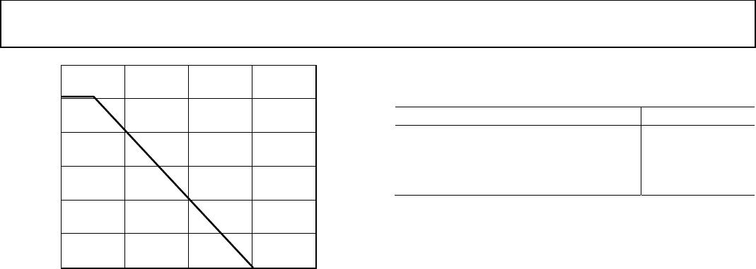
AMBIENT TEMPERATURE (°C)
SAFE LIMITING POWER (W)
0
0
1.2
1.0
0.8
0.6
0.4
0.2
50 100 150 200
15493-002
Figure 2. ADuM4120/ADuM4120-1 Thermal Derating Curve, Dependence of
Safety-Limiting Values on Case Temperature, per DIN V VDE V 0884-10
RECOMMENDED OPERATING CONDITIONS
Table 6.
Parameter Value
Operating Temperature Range (T
A
) −40°C to +125°C
Supply Voltages
V
DD1
− GND
1
or GND
2
2.5 V to 6.5 V
V
DD2
V
SS2
2
4.5 V to 35 V

ADUM4120-1ARIZ

Mfr. #:
Manufacturer:
Analog Devices Inc.
Description:
Gate Drivers Iso Gate Drvr w/2A output
Lifecycle:
New from this manufacturer.
Delivery:
DHL FedEx Ups TNT EMS
Payment:
T/T Paypal Visa MoneyGram Western Union