1
©
AUGUST 2013
CMOS SyncFIFO
64 x 9, 256 x 9, 512 x 9,
1,024 x 9, 2,048 x 9,
4,096 x 9 and 8,192 x 9
IDT and the IDT logo are registered trademarks of Integrated Device Technology, Inc. The SyncFIFO is a registered trademark of Integrated Device Technology, Inc.
COMMERCIAL AND INDUSTRIAL TEMPERATURE RANGES
IDT72421, IDT72201
IDT72211, IDT72221
IDT72231, IDT72241
IDT72251
2013 Integrated Device Technology, Inc. All rights reserved. Product specifications subject to change without notice. DSC-2655/6
FEATURES:
64 x 9-bit organization (IDT72421)
256 x 9-bit organization (IDT72201)
512 x 9-bit organization (IDT72211)
1,024 x 9-bit organization (IDT72221)
2,048 x 9-bit organization (IDT72231)
4,096 x 9-bit organization (IDT72241)
8,192 x 9-bit organization (IDT72251)
10 ns read/write cycle time
Read and Write Clocks can be independent
Dual-Ported zero fall-through time architecture
Empty and Full Flags signal FIFO status
Programmable Almost-Empty and Almost-Full flags can be set
to any depth
Programmable Almost-Empty and Almost-Full flags default to
Empty+7, and Full-7, respectively
Output enable puts output data bus in high-impedance state
Advanced submicron CMOS technology
Available in the 32-pin plastic leaded chip carrier (PLCC) and
32-pin Thin Quad Flat Pack (TQFP)
For through-hole product please see the IDT72420/72200/72210/
72220/72230/72240 data sheet
Industrial temperature range (–40
°°
°°
°C to +85
°°
°°
°C) is available
Green parts available, see ordering information
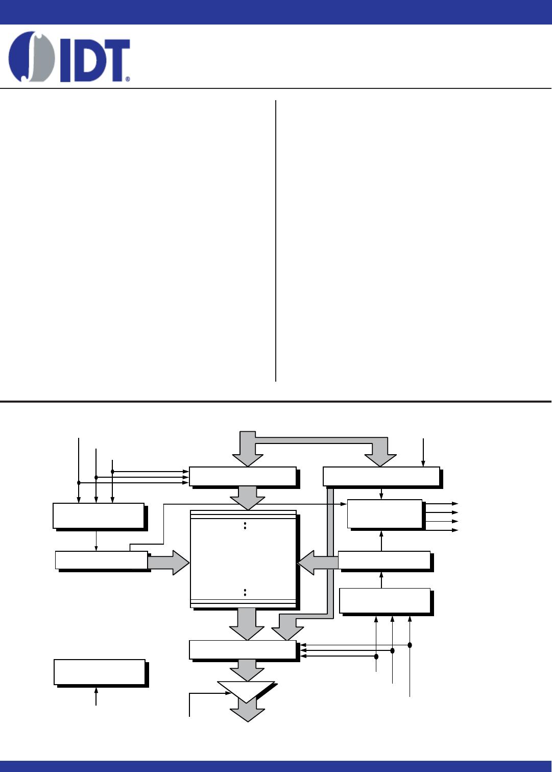
FUNCTIONAL BLOCK DIAGRAM
WCLK
WEN1
WEN2
D
0 - D8
LD
OFFSET REGISTER
INPUT REGISTER
RAM ARRAY
64 x 9, 256 x 9,
512 x 9, 1,024 x 9,
2,048 x 9, 4,096 x 9,
8,192 x 9
WRITE CONTROL
LOGIC
WRITE POINTER
OUTPUT REGISTER
READ CONTROL
LOGIC
READ POINTER
FLAG
LOGIC
EF
PAE
PAF
FF
RESET LOGIC
OE
REN2
REN1
RS
RCLK
2655 drw01
Q0 - Q8
DESCRIPTION:
The IDT72421/72201/72211/72221/72231/72241/72251 SyncFIFO™
are very high-speed, low-power First-In, First-Out (FIFO) memories with
clocked read and write controls. These devices have a 64, 256, 512, 1,024,
2,048, 4,096, and 8,192 x 9-bit memory array, respectively. These FIFOs are
applicable for a wide variety of data buffering needs such as graphics, local area
networks and interprocessor communication.
These FIFOs have 9-bit input and output ports. The input port is controlled
by a free-running clock (WCLK), and two write enable pins (WEN1, WEN2).
Data is written into the Synchronous FIFO on every rising clock edge when
the write enable pins are asserted. The output port is controlled by another clock
pin (RCLK) and two read enable pins (REN1, REN2). The Read Clock can
be tied to the Write Clock for single clock operation or the two clocks can run
asynchronous of one another for dual-clock operation. An output enable pin
(OE) is provided on the read port for three-state control of the output.
The Synchronous FIFOs have two fixed flags, Empty (EF) and Full (FF).
Two programmable flags, Almost-Empty (PAE) and Almost-Full (PAF), are
provided for improved system control. The programmable flags default to
Empty+7 and Full-7 for PAE and PAF, respectively. The programmable flag
offset loading is controlled by a simple state machine and is initiated by asserting
the load pin (LD).
These FIFOs are fabricated using high-speed submicron CMOS technology.
COMMERCIAL AND INDUSTRIAL
TEMPERATURE RANGES
IDT72421/72201/72211/72221/72231/72241/72251 CMOS SyncFIFO™
64 x 9, 256 x 9, 512 x 9, 1,024 x 9, 2,048 x 9, 4,096 x 9 and 8,192 x 9
2
©
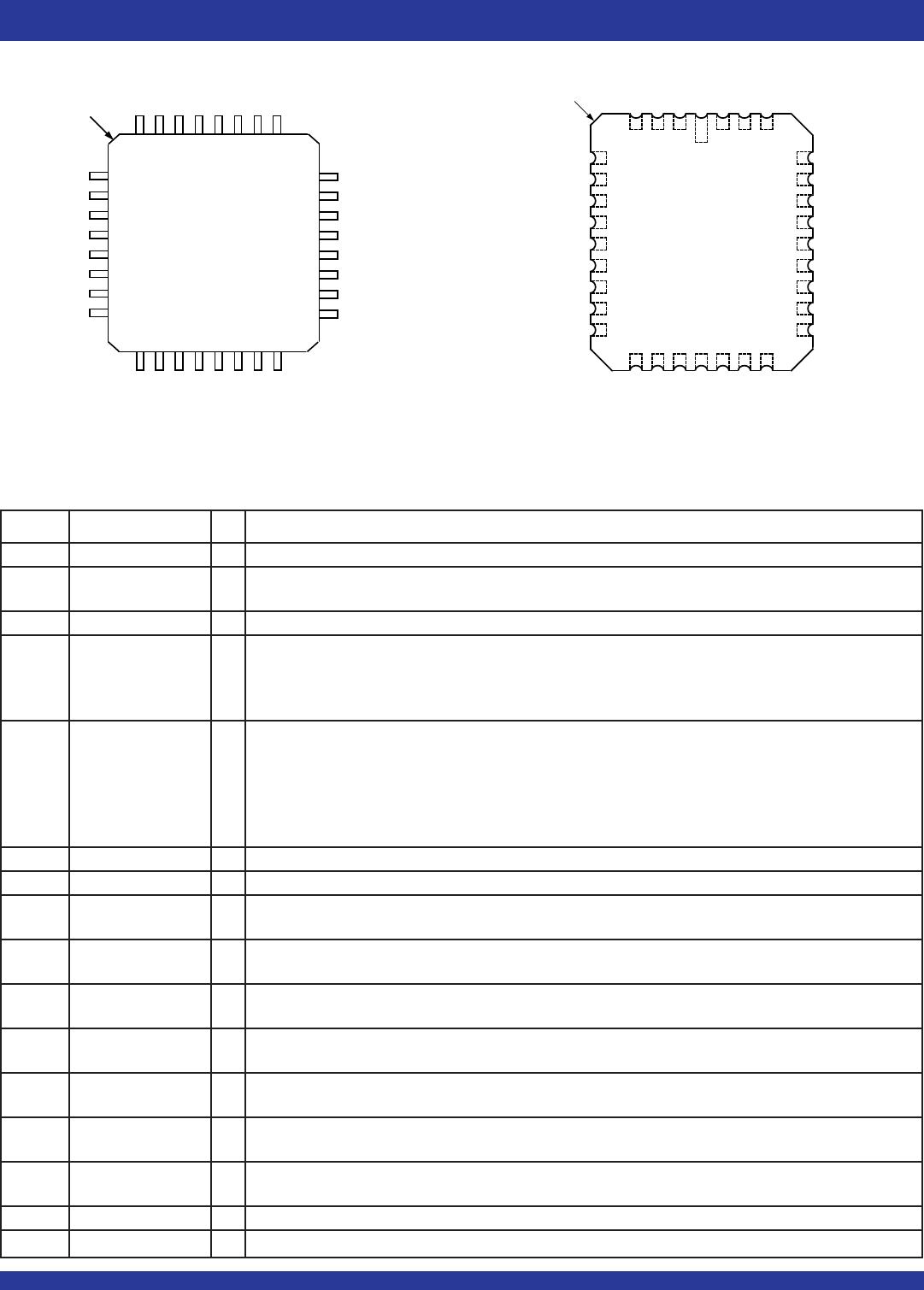
PIN CONFIGURATION
TQFP (PR32-1, order code: PF)
TOP VIEW
PLCC (J32-1, order code: J)
TOP VIEW
RS
WEN1
WCLK
WEN2/LD
5
6
7
8
16
V
CC
D
0
PAF
PAE
GND
REN1
RCLK
REN2
27 26 25
24
23
22
21
29 28
32 31 30
9 101112131415
2655 drw 02
EF
OE
FF
1
2
3
4
20
19
18
17
INDEX
D
1
Q
0
Q
1
Q
2
Q
3
Q
4
Q
8
Q
7
Q
6
Q
5
D
2
D
3
D
4
D
5
D
6
D
7
D
8
RS
WEN1
WCLK
WEN2/LD
V
CC
5
6
7
8
9
10
11
12
13
PAF
PAE
GND
REN1
RCLK
REN2
OE
27
26
25
24
23
22
21
29
28
432
1
32 31 30
14 15 16 17 18 19 20
D
2
FF
EF
INDEX
2655 drw02a
D
3
D
4
D
5
D
6
D
7
D
8
Q
0
Q
1
Q
2
Q
3
Q
4
Q
8
Q
7
Q
6
Q
5
D
1
D
0
Symbol Name I/O Description
D0-D8 Data Inputs I Data inputs for a 9-bit bus.
RS Reset I When RS is set LOW, internal read and write pointers are set to the first location of the RAM array,FF and PAF
go HIGH, and PAE and EF go LOW. A reset is required before an initial WRITE after power-up.
WCLK Write Clock I Data is written into the FIFO on a LOW-to-HIGH transition of WCLK when the Write Enable(s) are asserted.
WEN1 Write Enable 1 I If the FIFO is configured to have programmable flags, WEN1 is the only write enable pin. When WEN1 is LOW,
data is written into the FIFO on every LOW-to-HIGH transition WCLK. If the FIFO is configured to have two write
enables, WEN1 must be LOW and WEN2 must be HIGH to write data into the FIFO. Data will not be written into
the FIFO if the FF is LOW.
WEN2/ Write Enable 2/ I The FIFO is configured at reset to have either two write enables or programmable flags. If WEN2/LD is HIGH
LD
Load at reset, this pin operates as a second write enable. If WEN2/LD is LOW at reset, this pin operates as a control
to load and read the programmable flag offsets. If the FIFO is configured to have two write enables, WEN1 must
be LOW and WEN2 must be HIGH to write data into the FIFO. Data will not be written into the FIFO if the FF is
LOW. If the FIFO is configured to have programmable flags, WEN2/LD is held LOW to write or read the
programmable flag offsets.
Q0-Q8 Data Outputs O Data outputs for a 9-bit bus.
RCLK Read Clock I Data is read from the FIFO on a LOW-to-HIGH transition of RCLK when REN1 and REN2 are asserted.
REN1 Read Enable 1 I When REN1 and REN2 are LOW, data is read from the FIFO on every LOW-to-HIGH transition of RCLK.
Data will not be read from the FIFO if the EF is LOW.
REN2 Read Enable 2 I When REN1 and REN2 are LOW, data is read from the FIFO on every LOW-to-HIGH transition of RCLK.
Data will not be read from the FIFO if the EF is LOW.
OE Output Enable I When OE is LOW, the data output bus is active. If OE is HIGH, the output data bus will be in a high-impedance
state.
EF Empty Flag O When EF is LOW, the FIFO is empty and further data reads from the output are inhibited. When EF is HIGH, the
FIFO is not empty. EF is synchronized to RCLK.
PAE Programmable O When PAE is LOW, the FIFO is almost-empty based on the offset programmed into the FIFO. The default
Almost-Empty Flag offset at reset is Empty+7. PAE is synchronized to RCLK.
PAF Programmable O When PAF is LOW, the FIFO is almost-full based on the offset programmed into the FIFO. The default offset
Almost-Full Flag at reset is Full-7. PAF is synchronized to WCLK.
FF Full Flag O When FF is LOW, the FIFO is full and further data writes into the input are inhibited. When FF is HIGH, the FIFO
is not full. FF is synchronized to WCLK.
VCC Power One +5 volt power supply pin.
GND Ground One 0 volt ground pin.
PIN DESCRIPTIONS
3
©
COMMERCIAL AND INDUSTRIAL
TEMPERATURE RANGES
IDT72421/72201/72211/72221/72231/72241/72251 CMOS SyncFIFO™
64 x 9, 256 x 9, 512 x 9, 1,024 x 9, 2,048 x 9, 4,096 x 9 and 8,192 x 9
IDT72421
IDT72201
IDT72211
IDT72221
IDT72231
IDT72241 IDT72251
Com'l and Ind'l
(1)
Com'l and Ind'l
(1)
tCLK = 10, 15, 25 ns tCLK = 10, 15, 25 ns
Symbol Parameter Min. Typ. Max. Min. Typ. Max. Unit
ILI
(2)
Input Leakage Current (Any Input) –1 1 –1 1 μA
ILO
(3)
Output Leakage Current –10 10 –10 10 μA
VOH
Output Logic “1” Voltage, IOH = –2mA
2.4 2.4 V
VOL Output Logic “0” Voltage, IOL = 8mA 0.4 0.4 V
ICC1
(4,5,6)
Active Power Supply Current 35 50 mA
ICC2
(4,7)
Standby Current 5 5 mA
NOTES:
1. Industrial temperature range product for the 15ns and 25ns speed grades are available as standard product.
2. Measurements with 0.4
VIN
VCC.
3. OE VIH, 0.4 VOUT VCC.
4. Tested with outputs open (IOUT = 0).
5. RCLK and WCLK toggle at 20 MHz and data inputs switch at 10 MHz.
6. Typical ICC1 = 1.7 + 0.7*fS + 0.02*CL*fS (in mA).
These equations are valid under the following conditions:
VCC = 5V, TA = 25°C, fS = WCLK frequency = RCLK frequency (in MHz, using TTL levels), data switching at fS/2, CL = capacitive load (in pF).
7. All Inputs = VCC - 0.2V or GND + 0.2V, except RCLK and WCLK, which toggle at 20 MHz.
DC ELECTRICAL CHARACTERISTICS
(Commercial: V
CC
= 5V ± 10%, T
A
= 0
°
C to +70
°
C; Industrial: V
CC
= 5V ± 10%, T
A
= –40
°
C to +85
°
C)
Symbol Rating Com'l & Ind'l Unit
V
TERM Terminal Voltage with –0.5 to +7.0 V
Respect to GND
T
STG Storage Temperature –55 to +125 °C
I
OUT DC Output Current –50 to +50 mA
Symbol Parameter Min. Typ. Max. Unit
V
CC Supply Voltage 4.5 5.0 5.5 V
Commercial/Industrial
GND Supply Voltage 0 0 0 V
V
IH Input High Voltage 2.0 V
Commercial/Industrial
V
IL Input Low Voltage 0.8 V
Commercial/Industrial
TA Operating Temperature 0 +70 °C
Commercial
TA Operating Temperature –40 +85 °C
Industrial
NOTE:
1. Stresses greater than those listed under ABSOLUTE MAXIMUM RATINGS may cause
permanent damage to the device. This is a stress rating only and functional operation
of the device at these or any other conditions above those indicated in the operational
sections of the specification is not implied. Exposure to absolute maximum rating
conditions for extended periods may affect reliability.
ABSOLUTE MAXIMUM RATINGS
RECOMMENDED OPERATING
CONDITIONS

72251L15PFGI

Mfr. #:
Manufacturer:
IDT
Description:
FIFO 8K X 9 SYNCFIFO
Lifecycle:
New from this manufacturer.
Delivery:
DHL FedEx Ups TNT EMS
Payment:
T/T Paypal Visa MoneyGram Western Union