11
©
COMMERCIAL AND INDUSTRIAL
TEMPERATURE RANGES
IDT72421/72201/72211/72221/72231/72241/72251 CMOS SyncFIFO™
64 x 9, 256 x 9, 512 x 9, 1,024 x 9, 2,048 x 9, 4,096 x 9 and 8,192 x 9
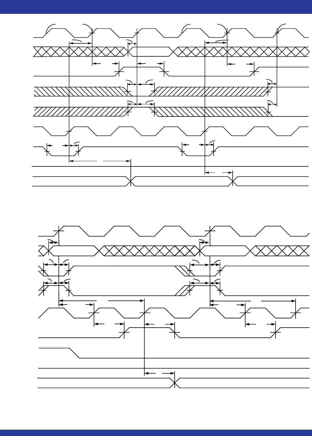
Figure 11. Programmable Empty Flag Timing
NOTES:
1. n = PAE offset.
2. tSKEW2 is the minimum time between a rising WCLK edge and a rising RCLK edge for PAE to change during that clock cycle. If the time between the rising edge of WCLK and
the rising edge of RCLK is less than tSKEW2, then PAE may not change state until the next RCLK rising edge.
3. If a read is performed on this rising edge of the Read Clock, there will be Empty + (n-1) words in the FIFO when PAE goes LOW.
NOTES:
1. m = PAF offset .
2. 64-m words in FIFO for IDT72421, 256-m words for IDT72201, 512-m words for IDT72211, 1,024-m words for IDT72221, 2,048-m words for IDT72231, 4,096-m words for IDT72241,
and 8,192-m words for IDT72251.
3. tSKEW2 is the minimum time between a rising RCLK edge and a rising WCLK edge for PAF to change during that clock cycle. If the time between the rising edge of RCLK and
the rising edge of WCLK is less than tSKEW2, then PAF may not change state until the next WCLK rising edge.
4. If a write is performed on this rising edge of the Write Clock, there will be Full - (m-1) words in the FIFO when PAF goes LOW.
Figure 10. Programmable Full Flag Timing
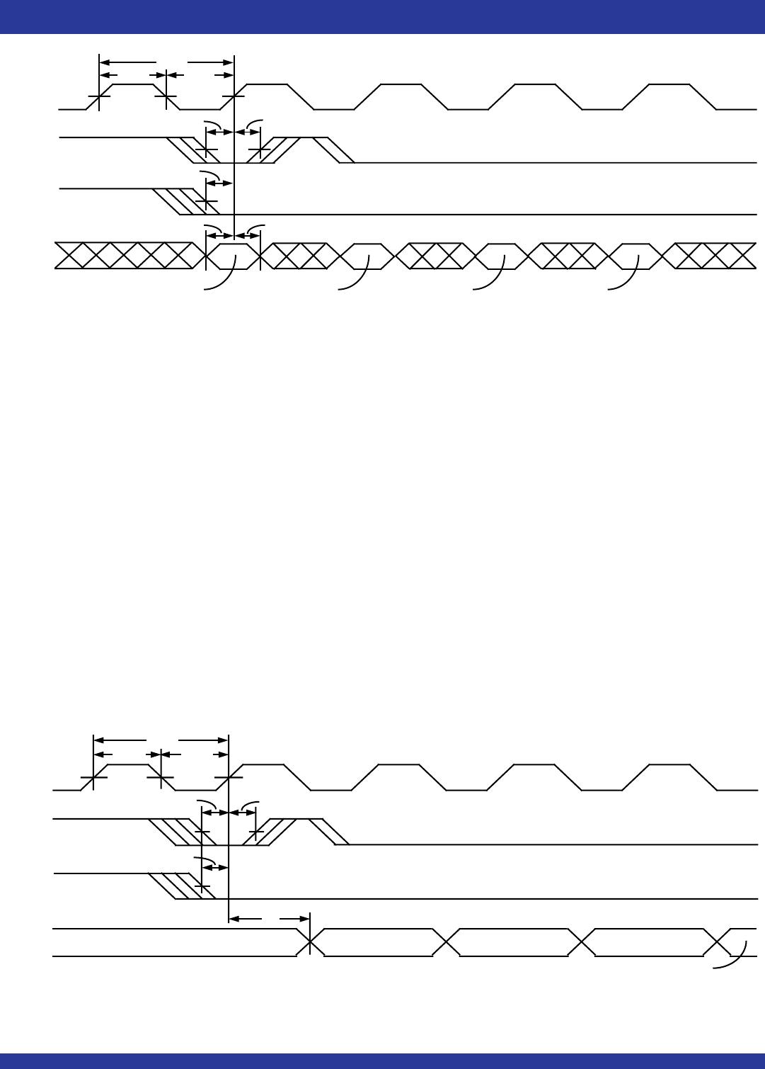
t
ENS
t
ENH
t
ENS
t
ENH
t
ENS
t
ENH
WCLK
WEN1
WEN2
(If Applicable)
PAF
RCLK
REN1,
REN2
(4)
(1)
t
PAF
Full - (m+1) words in FIFO
Full - m words in FIFO
(2)
t
CLKH
t
CLKL
t
SKEW2
(3)
t
PAF
2655 drw 12
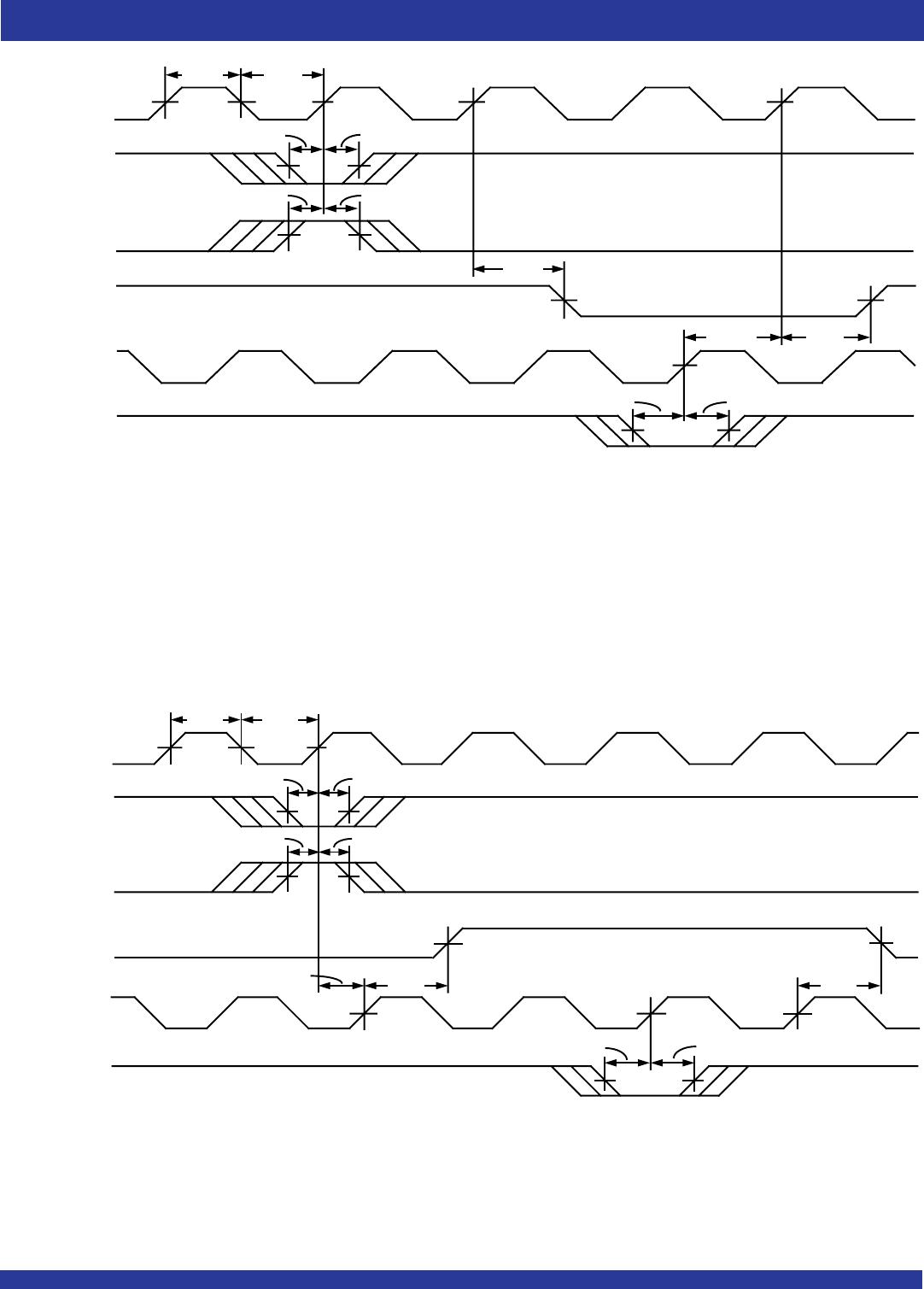
WCLK
WEN1
WEN2
PAE
RCLK
REN1,
REN2
t
ENS
t
ENH
t
ENS
t
ENH
t
SKEW2
(2)
t
ENS
t
ENH
(If Applicable)
t
PAE
t
PAE
(3)
(1)
n words in FIFO
n+1 words in FIFO
t
CLKH
t
CLKL
2655 drw 13