LTC6820
15
6820fb
For more information www.linear.com/LTC6820
OPERATION
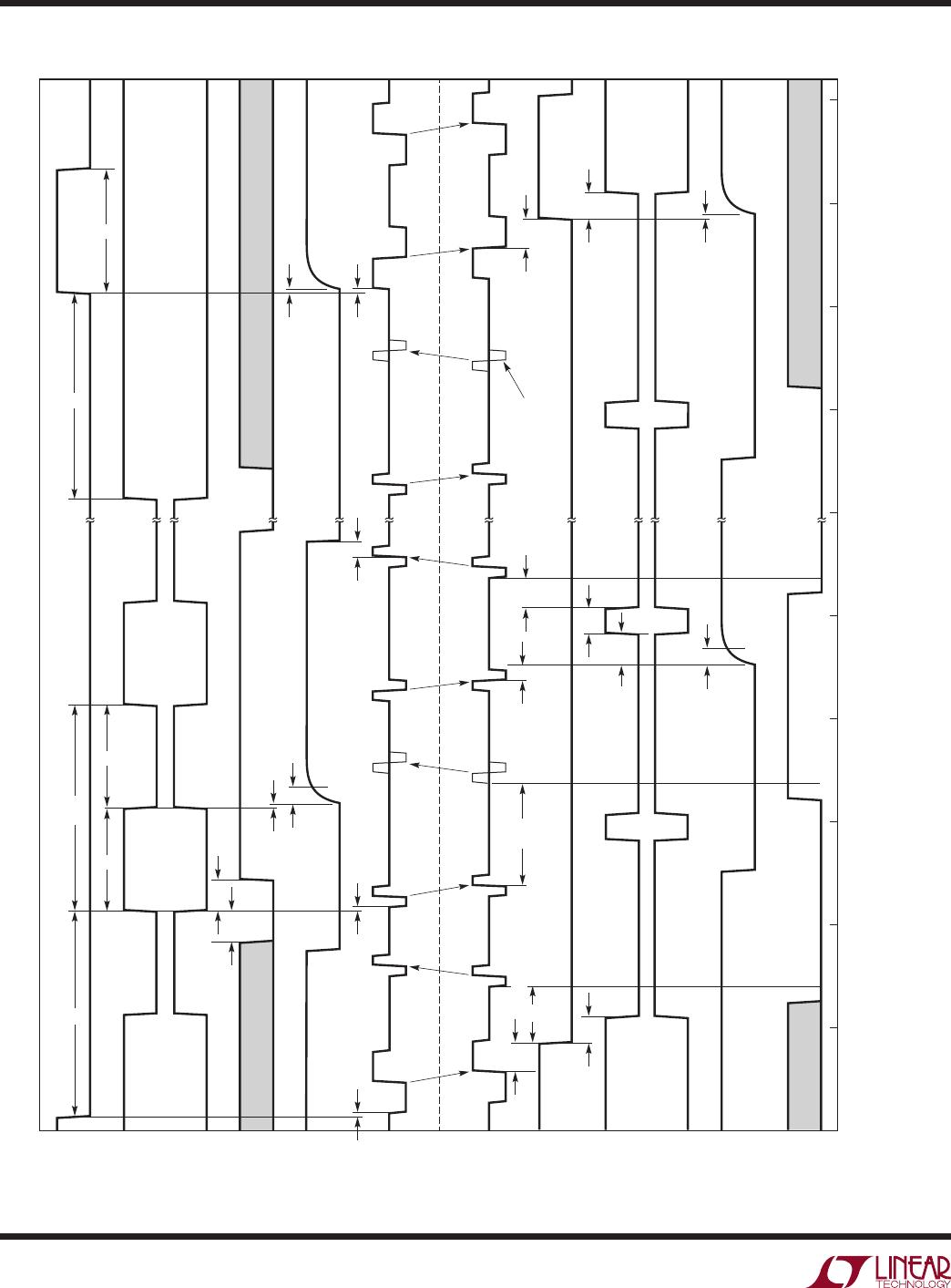
Figure 6 demonstrates slow mode, as compared to fast
mode in Figure 5.
Figure 5. Fast Mode (SLOW = 0)
Figure 6. Slow Mode (SLOW = 1)
IP-IM
2V/DIV
SCK
5V/DIV
MOSI
5V/DIV
MISO
5V/DIV
200ns/DIV
6820 F05
V
DD
= 5V
V
DDS
= 5V
IP-IM
2V/DIV
SCK
5V/DIV
MOSI
5V/DIV
MISO
5V/DIV
1µs/DIV
6820 F06
V
DD
= 5V
V
DDS
= 5V
IP and IM Pulse Driver
The IP and IM pins transmit and receive the isoSPI pulses.
The transmitter uses a current-regulated driver (see
Figure7) to establish the pulse amplitude, as determined
by the IBIAS pin current, I
B
, and the load resistance. The
sinking current source is regulated to 20x the bias current I
B
.
The sourcing current source operates in a current-starved
(resistive) manner to maintain the sourcing pin’s voltage
near V
DD
, as shown in Figures 8 and 9. The common mode
voltage (while driving) is dependent on bias current and
output amplitude.
The output driver will regulate the common mode and
peak swing of IP and IM to the proper levels, allowing for
a broad range of output amplitude with fairly flat gain, as
shown in Figure 10.
+
–
R
M
35k
OPEN WHEN IDLE
+ 167mV
V
DD
V
DD
35k
6820 F07
POS
NEG
20 • I
B
POS
NEG
V
IP
– V
IM
IP
V
ICMP
3
IM
Figure 7. Pulse Driver
V
IP
OR V
IM
(V)
0
0
SOURCE/SINK CURRENT (mA)
5
10
15
20
25
0.5
1 1.5 2
6820 F08
2.5 3
SOURCING OUTPUT
1V AMPLITUDE
SINKING OUTPUT
V
DD
= 3V
I
B
= 1mA
Figure 8. Drive Source/Sink vs Output Voltage
PULSE AMPLITUDE (V)
0
0
OUTPUT VOLTAGE (V)
0.5
1.0
1.5
2.0
3.0
V
CM
0.5
1 1.5 2
6820 F09
2.5 3
2.5
SOURCING
OUTPUT
SINKING
OUTPUT
V
DD
= 3V
I
B
= 1mA
Figure 9. Output Voltages and Common Mode vs Amplitude