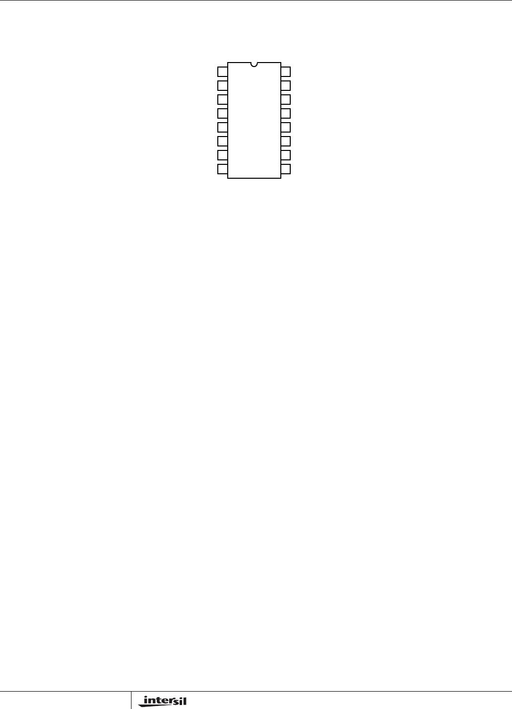
1
®
FN7175.4
EL4585
Horizontal Genlock, 8F
SC
The EL4585 is a PLL (Phase Lock Loop) sub-system,
designed for video applications and also suitable for general
purpose use up to 36MHz. In video applications, this device
generates a TTL/CMOS-compatible pixel clock (CLK OUT)
which is a multiple of the TV horizontal scan rate and phase
locked to it.
The reference signal is a horizontal sync signal, TTL/CMOS
format, which can be easily derived from an analog
composite video signal with the EL4583 sync separator. An
input signal to “coast” is provided for applications where
periodic disturbances are present in the reference video
timing such as VTR head switching. The lock detector output
indicates correct lock.
The divider ratio is four ratios for NTSC and four similar
ratios for the PAL video timing standards by external
selection of three control pins. These four ratios have been
selected for common video applications including 8F
SC
,
6F
SC
, 27MHz (CCIR 601 format) and square picture
elements used in some workstation graphics. To generate
4F
SC
, 3F
SC
, 13.5MHz (CCIR 601 format) etc., use the
EL4584, which does not have the additional divide-by-two
stage of the EL4585.
For applications where these frequencies are inappropriate
or for general purpose PLL applications the internal divider
can be bypassed and an external divider chain used.
Features
• 36MHz, general purpose PLL
•8F
SC
timing (use the EL4584 for 4F
SC
)
• Compatible with EL4583 sync separator
• VCXO, Xtal, or LC tank oscillator
• < 2ns jitter (VCXO)
• User-controlled PLL capture and lock
• Compatible with NTSC and PAL TV formats
• 8 pre-programmed popular TV scan rate clock divisors
• Single 5V, low current operation
• Pb-Free Available (RoHS Compliant)
Applications
• Pixel clock regeneration
• Video compression engine (MPEG) clock generator
• Video capture or digitization
• PIP (Picture in Picture) timing generator
• Text or graphics overlay timing
Demo Board
A demo PCB is available for this product.
FREQUENCIES AND DIVISORS
FUNCTION
6F
SC
(Note 1)
CCIR 601
(Note 2)
SQUARE
(Note 3) 8F
SC
Divisor (Note 4) 1702 1728 1888 2270
PAL F
OSC
(MHz) 26.602 27.0 29.5 35.468
Divisor (Note 4) 1364 1716 1560 1820
NTSC F
OSC
(MHz) 21.476 27.0 24.546 28.636
NOTES:
1. 6F
SC
frequencies do not yield integer divisors.
2. CCIR 601 divisors yield 1440 pixels in the active portion of each
line for NTSC and PAL.
3. Square pixels format gives 640 pixels for NTSC and 768 pixels
for PAL.
4. Divisor does not include ÷ 2 block.
Ordering Information
PART
NUMBER
PART
MARKING PACKAGE
PKG.
DWG. #
EL4585CN EL4585CN 16 Ld PDIP E16.3
EL4585CS EL4585CS 16 Ld SOIC MDP0027
EL4585CS-T7* EL4585CS 16 Ld SOIC MDP0027
EL4585CS-T13* EL4585CS 16 Ld SOIC MDP0027
EL4585CSZ
(Note 5)
EL4585CSZ 16 Ld SOIC
(Pb-free)
MDP0027
EL4585CSZ-T7*
(Note 5)
EL4585CSZ 16 Ld SOIC
(Pb-free)
MDP0027
EL4585CSZ-T13*
(Note 5)
EL4585CSZ 16 Ld SOIC
(Pb-free)
MDP0027
*Please refer to TB347 for details on reel specifications.
NOTES:
5. These Intersil Pb-free plastic packaged products employ special
Pb-free material sets, molding compounds/die attach materials,
and 100% matte tin plate plus anneal (e3 termination finish,
which is RoHS compliant and compatible with both SnPb and
Pb-free soldering operations). Intersil Pb-free products are
MSL classified at Pb-free peak reflow temperatures that meet
or exceed the Pb-free requirements of IPC/JEDEC J STD-020.
6. For 3F
SC
and 4F
SC
clock frequency operation, see EL4584
datasheet.
Data Sheet September 3, 2009
CAUTION: These devices are sensitive to electrostatic discharge; follow proper IC Handling Procedures.
1-888-INTERSIL or 1-888-468-3774
| Intersil (and design) is a registered trademark of Intersil Americas Inc.
Copyright Intersil Americas Inc. 2003-2005, 2009. All Rights Reserved
All other trademarks mentioned are the property of their respective owners.


