8
FN7175.4
September 3, 2009
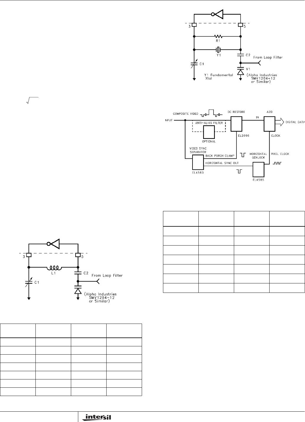
varactor within this range. Crystal oscillators are more stable
than LC oscillators, which translates into lower jitter, but LC
oscillators can be pulled from their mid-point values further,
resulting in a greater capture and locking range. If the
incoming horizontal sync signal is known to be very stable,
then a crystal oscillator circuit can be used. If the H
SYNC
signal experiences frequency variations of greater than
about 300ppm, an LC oscillator should be considered, as
crystal oscillators are very difficult to pull this far. When
H
SYNC
input frequency is greater than CLK frequency ÷ 2N,
charge pump output (pin 7) sources current into the filter
capacitor, increasing the voltage across the varactor, thus
tending to increase VCO frequency. Conversely, charge
pump output pulls current from the filter capacitor when
H
SYNC
frequency is less than CLK ÷ 2N, forcing the VCO
frequency lower.
Loop Filter
The loop filter controls how fast the VCO will respond to a
change in phase comparator output stimulus. Its
components should be chosen so that fast lock can be
achieved, yet with a minimum of VCO “hunting”, preferably in
one to two oscillations of charge pump output, assuming the
VCO frequency starts within capture range. If the filter is
under-damped, the VCO will over and under-shoot the
desired operating point many times before a stable lock
takes place. It is possible to under-damp the filter so much
that the loop itself oscillates, and VCO lock is never
achieved. If the filter is over-damped, the VCO response
time will be excessive and many cycles will be required for a
lock condition. Over-damping is also characterized by an
easily unlocked system because the filter can’t respond fast
enough to perturbations in VCO frequency. A severely over
damped system will seem to endlessly oscillate, like a very
large mass at the end of a long pendulum. Due to parasitic
effects of PCB traces and component variables, it will take
some trial and error experimentation to determine the best
values to use for any given situation. Use the component
tables as a starting point, but be aware that deviations from
these values are not out of the ordinary.
External Divide
DIV SEL (pin 8) controls the use of the internal divider. When
high, the internal divider is enabled and EXT DIV (pin 13)
outputs the CLK out divided by 2N. This is the signal to
which the horizontal sync input will lock. When divide select
is low, the internal divider output is disabled, and external
divide becomes an input from an external divider, so that a
divisor other than one of the 8 pre-programmed internal
divisors can be used.
Normal Mode
Normal mode is enabled by pulling COAST (pin 9) low
(below 1/3*V
CC
). If H
SYNC
and CLK ÷ 2N have any phase or
frequency difference, an error signal is generated and sent
to the charge pump. The charge pump will either force
current into or out of the filter capacitor in an attempt to
modulate the VCO frequency. Modulation will continue until
the phase and frequency of CLK ÷ 2N exactly match the
H
SYNC
input. When the phase and frequency match (with
some offset in phase that is a function of the VCO
characteristics), the error signal goes to zero, lock detect no
longer pulses high, and the charge pump enters a high
impedance state. The clock is now locked to the H
SYNC
input. As long as phase and frequency differences remain
small, the PLL can adjust the VCO to remain locked and lock
detect remains low.
Fast Lock Mode
Fast Lock mode is enabled by either allowing coast to float,
or pulling it to mid supply (between 1/3 and 2/3*V
CC
). In this
mode, lock is achieved much faster than in normal mode, but
the clock divisor is modified on the fly to achieve this. If the
phase detector detects an error of enough magnitude, the
clock is either inhibited or reset to attempt a “fast lock” of the
signals. Forcing the clock to be synchronized to the H
SYNC
input this way allows a lock in approximately 2 H-cycles, but
the clock spacing will not be regular during this time. Once
the near lock condition is attained, charge pump output
should be very close to its lock-on value, and placing the
device into normal mode should result in a normal lock very
quickly. Fast lock mode is intended to be used where H
SYNC
becomes irregular, until a stable signal is again obtained.
Coast Mode
Coast mode is enabled by pulling COAST (pin 9) high
(above 2/3*V
CC
). In coast mode the internal phase detector
is disabled and filter out remains in high impedance mode to
keep filter out voltage and VCO frequency as constant as
possible. VCO frequency will drift as charge leaks from the
filter capacitor, and the voltage changes the VCO operating
point. Coast mode is intended to be used when noise or
signal degradation result in loss of horizontal sync for many
cycles. The phase detector will not attempt to adjust to the
resultant loss of signal so that when horizontal sync returns,
sync lock can be re-established quickly. However, if much
VCO drift has occurred, it may take as long to re-lock as
when restarting.
Lock Detect
Lock detect (pin 12) will go low when lock is established. Any
DC current path from charge pump out will skew EXT DIV
relative to HSYNC in, tending to offset or add to the 200ns
internal delay, depending on which way the extra current is
flowing. This offset is called static phase error, and is always
present in any PLL system. If, when the part stabilizes in a
locked mode, lock detect is not low, adding or subtracting
from the loop filter series resistor R2 will change this static
phase error to allow LDET to go low while in lock. The goal is
to put the rising edge of EXT DIV in sync with the falling
edge of HSYNC + 200ns (see “Timing Diagrams” on
page 5). Increasing R2 decreases phase error, while
decreasing R2 increases phase error. (Phase error is
EL4585