10
FN7175.4
September 3, 2009
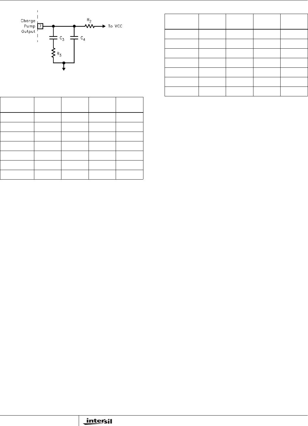
C
1
is to adjust the center frequency, C
2
DC isolates the
control from the oscillator, and V
1
is the primary control
device. C
2
should be much larger than C
V
so that V
1
has
maximum modulation capability. The frequency of oscillation
is given by Equation 4:
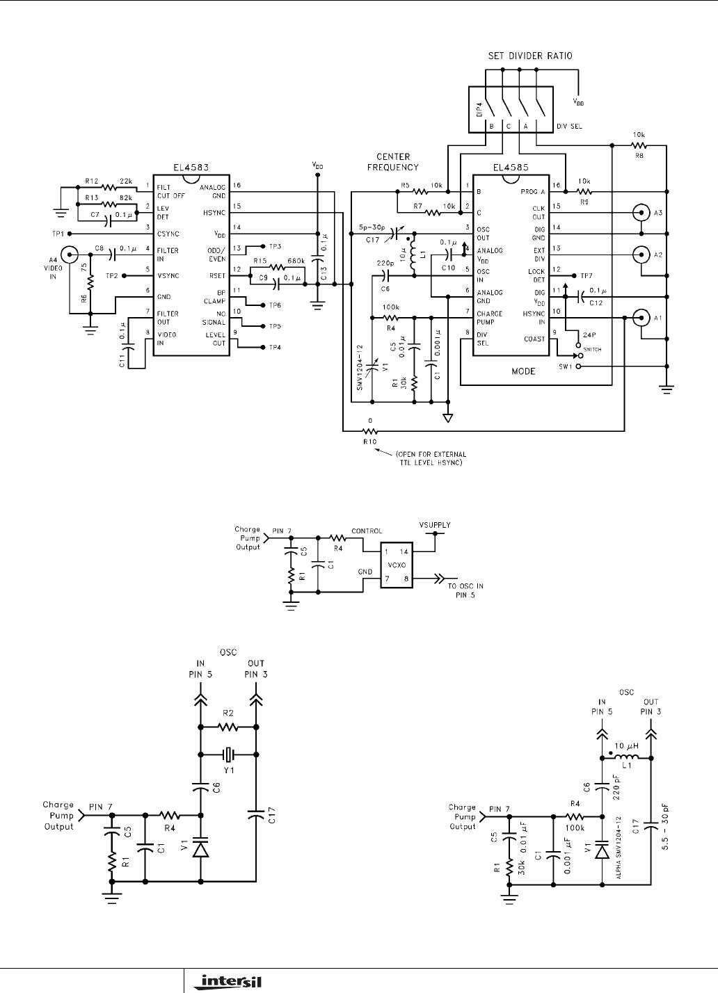
Choosing Loop Filter Components
The PLL, VCO, and loop filter can be described as:
Where:
K
d
= phase detector gain in A/rad
F(s) = loop filter impedance in V/A
K
VCO
= VCO gain in rad/s/V
N = Total internal or external divisor (see 3 below)
It can be shown that for the loop filter shown in Equation 5:
Where ω
n
= loop filter bandwidth, and ζ = loop filter damping
factor.
1. K
d
= 300µA/2πrad = 4.77e-5A/rad for the EL4585.
2. The loop bandwidth should be about H
SYNC
frequency/20, and the damping ratio should be 1 for
optimum performance. For our example,
ω
n
= 15.734kHz/20=787 Hz≈5000 rad/S.
3. N = 910x2 = 1820 from Table 1.
4. K
VCO
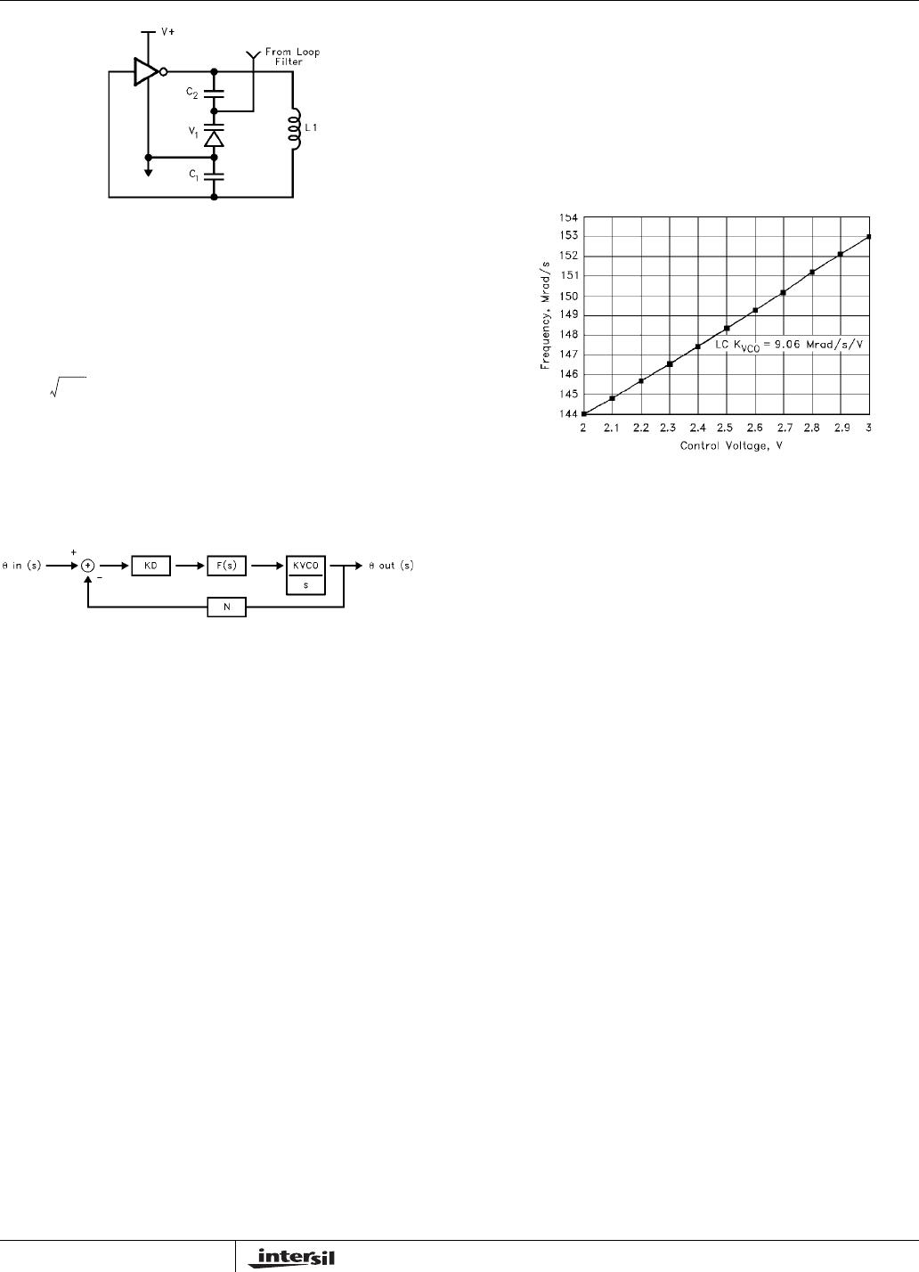
represents how much the VCO frequency changes
for each volt applied at the control pin. It is assumed (but
probably is not) linear about the lock point (2.5V). Its
value depends on the VCO configuration and the varactor
transfer function C
V
=F(V
C
), where V
C
is the reverse
bias control voltage, and C
V
is varactor capacitance.
Since F(V
C
) is nonlinear, it is probably best to build the
VCO and measure K
VCO
about 2.5V. The results of one
such measurement are shown below. The slope of the
curve is determined by linear regression techniques and
equals K
VCO
. For our example, K
VCO
= 9.06 Mrad/s/V.
5. Now we can solve for C
3
, C
4
, and R
3
in Equation 7:
We choose R
3
= 43kΩ for convenience.
6. Notice R
2
has little effect on the loop filter design. R
2
should be large, around 100k, and can be adjusted to
compensate for any static phase error Tθ at lock, but if
made too large, will slow loop response. If R
2
is made
smaller, Tθ (see “Timing Diagrams” on page 5) increases,
and if R
2
increases, Tθ decreases. For LDET to be low at
lock, |Tθ| < 50ns. C
4
is used mainly to attenuate high
frequency noise from the charge pump. The effect these
components have on-time to lock is illustrated in
Figure 12.
Lock Time
Let T = R
3
C
3
. As T increases, damping increases, but so
does lock time. Decreasing T decreases damping and
speeds up loop response, but increases overshoot and thus
increases the number of hunting oscillations before lock.
Critical damping (ζ=1) occurs at minimum lock time.
Because decreased damping also decreases loop stability, it
is sometimes desirable to design slightly overdamped (ζ>1),
trading lock time for increased stability.
FIGURE 10. COLPITTS OSCILLATOR
F
1
2π LC
T
-----------------------
=
C
T
C
1
C
2
C
v
C
1
C
2
()C
1
C
V
()C
1
C
V
()++
--------------------------------------------------------------------------
=
(EQ. 4)
C
3
K
d
K
VCO
Nω
n
2
------------------------
C
4
,
C
3
10
-------
R
3
,
2Nζω
n
K
d
K
VCO
------------------------
===
(EQ. 5)
N
F
VCO
F
Hsync
--------------------
28.636M
15.73426k
----------------------------
1820 910x2== ==
(EQ. 6)
FIGURE 11. FOSC vs VC, LC VCO
C
3
K
d
K
VCO
Nω
n
2
------------------------
4.77e 5–()9.06e6()
1820()5000()
2
------------------------------------------------------
0.01μF== =
C
4
C
3
10
-------
0.001μF==
R
3
2Nζω
2
K
d
K
VCO
------------------------
2()1820()1()5000()
4.77e 5–()9.06e6()
------------------------------------------------------
42.1kΩ== =
(EQ. 7)
EL4585