4
FN7175.4
September 3, 2009
Pin Descriptions
Pin NUMBER PIN NAME FUNCTION
1, 2, 16 PROG B, C, A Digital inputs to select ÷ N value for internal counter. See Table 1 for values.
3 OSC/VCO OUT Output of internal inverter/oscillator. Connect to external crystal or LC tank VCO circuit.
4 VDD (A) Analog positive supply for oscillator, PLL circuits.
5 OSC/VCO IN Input from external VCO.
6 VSS (A) Analog ground for oscillator, PLL circuits.
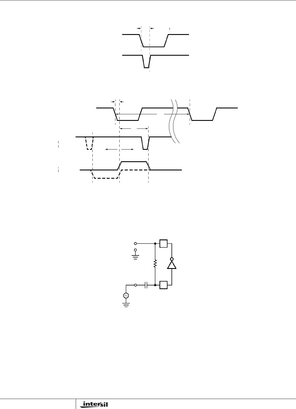
7 CHARGE PUMP
OUT
Connect to loop filter. If the H
SYNC
phase is leading or H
SYNC
frequency > CLK ÷ 2N, current is pumped
into the filter capacitor to increase VCO frequency. If H
SYNC
phase is lagging or frequency < CLK ÷ 2N,
current is pumped out of the filter capacitor to decrease VCO frequency. During coast mode or when
locked, charge pump goes to a high impedance state.
8 DIV SELECT Divide select input. When high, the internal divider is enabled and EXT DIV becomes a test pin, outputting
CLK ÷ 2N. When low, the internal divider is disabled and EXT DIV is an input from an external ÷N.
9 COAST Three-state logic input. Low (< 1/3*V
CC
) = normal mode, Hi Z (or 1/3 to 2/3*V
CC
) = fast lock mode,
High (> 2/3*V
CC
) = coast mode.
10 HSYNC IN Horizontal sync pulse (CMOS level) input.
11 VDD (D) Positive supply for digital, I/O circuits.
12 LOCK DET Lock detect output. Low level when PLL is locked. Pulses high when out of lock.
13 EXT DIV External divide input when DIV SEL is low, internal ÷ 2N output when DIV SEL is high.
14 VSS (D) Ground for digital, I/O circuits.
15 CLK OUT Buffered output of the VCO.
TABLE 1. VCO DIVISORS
PROG A (PIN 16) PROG B (PIN 1) PROG C (PIN 2) DIV VALUE (N)
0 0 0 1702
0 0 1 1728
0 1 0 1888
0 1 1 2270
1 0 0 1364
1 0 1 1716
1 1 0 1560
1 1 1 1820
EL4585