10
FN6514.2
October 30, 2007
A microprocessor or a switch can be used to drive the HP
pin rather than using the headphone jack contact pin.
Note: With a logic “1” at the HO pin, the BTL driver remains
active regardless of the voltage level at the HD pin. This
allows a headphone to be plugged into the headphone jack
without activating the HP drivers. Music will continue to play
through the internal 8 speaker rather than the headphones.
Low Power Shutdown
With a logic “1” at the SD control pin the device enters the
low power shutdown state. When in shutdown the BTL and
headphone amplifiers go into an high impedance state and
I
DD
supply current is reduced to 26µA (typ).
In shutdown mode before the amplifiers enter the high
impedance/low current drive state, the bias voltage of V
DD
/2
remains connected at the output of the amplifiers through a
100k resistor.
This resistor is not present during active operation of the
drivers but gets switched in when the SD pin goes high. It
gets removed when the SD pin goes low.
Leaving the DC bias voltage connected through a 100k
resistor while going into and out of shutdown reduces the
transient at the speakers to a small level preventing clicking
or popping in the speakers.
Note: When the SD pin is High it over-rides all other logic
pins.
QFN Thermal Pad Considerations
The QFN package features an exposed thermal pad on its
underside. This pad lowers the package’s thermal resistance
by providing a direct heat conduction path from the die to the
PCB. Connect the exposed thermal pad to GND by using a
large copper pad and multiple vias to the GND plane. The
vias should be plugged and tented with plating and solder
mask to ensure good thermal conductivity.
Best thermal performance is achieved with the largest
practical copper ground plane area.
PCB Layout Considersations and Power
Supply Bypassing
To maintain the highest load dissipation and widest output
voltage swing, the power supply PCB traces and the traces
that connect the output of the drivers to the speaker loads
should be made as wide as possible to minimize losses due
to parasitic trace resistance.
Proper supply bypassing is necessary for high power supply
rejection and low noise performance. A filter network
consisting of a 10µF capacitor in parallel with a 0.1µF
capacitor is recommended at the voltage regulator that is
providing the power to the ISL54003, ISL54004, ISL54006
IC.
Local bypass capacitors of 0.1µF should be put at each VDD
pin of the ISL54003, ISL54004, ISL54006 devices. They
should be located as close as possible to the pin, keeping
the length of leads and traces as short as possible.
A 1µF capacitor from the REF pin (pin 10) to ground is
needed for optimum PSRR and internal bias voltage stability.
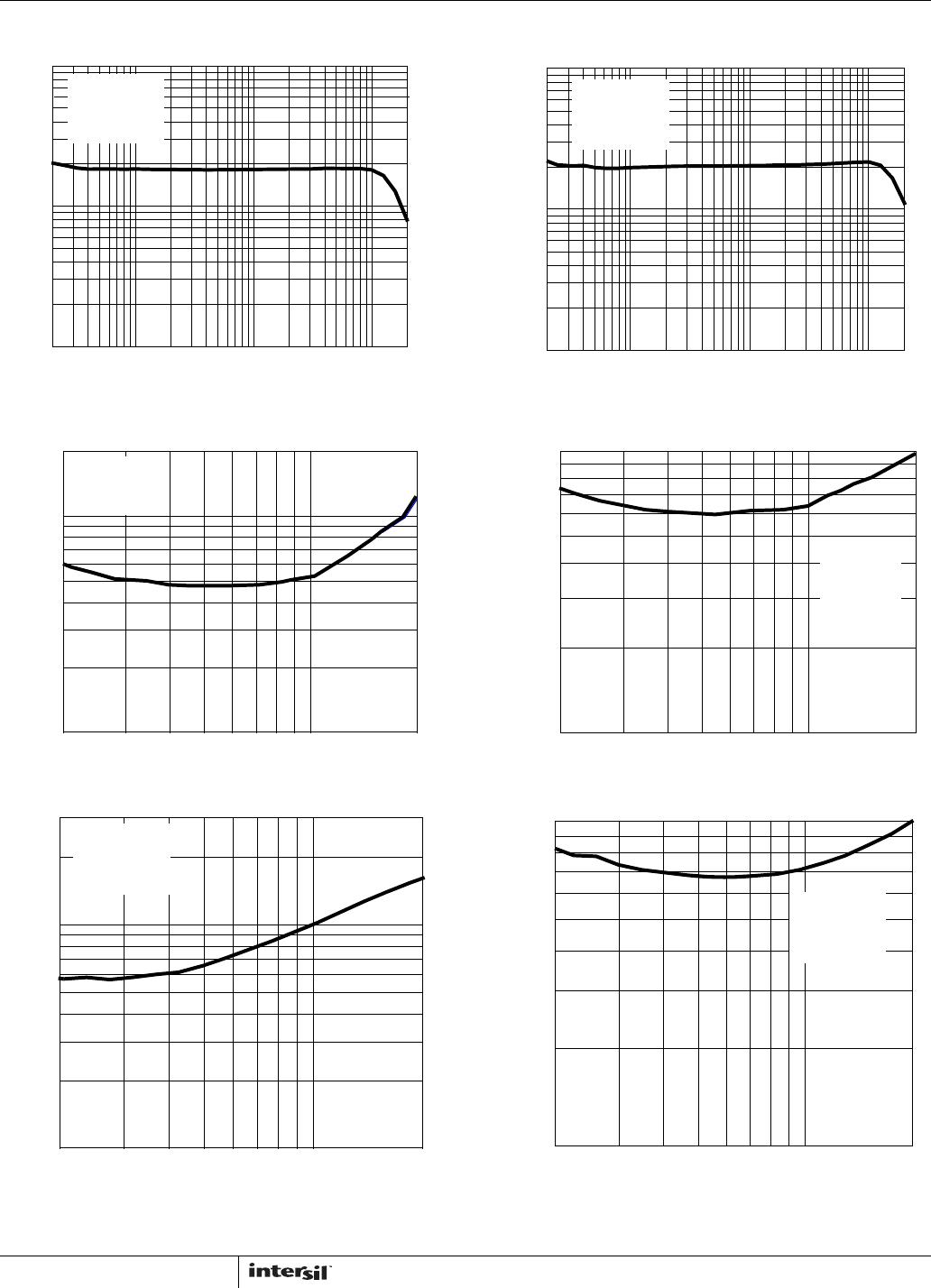
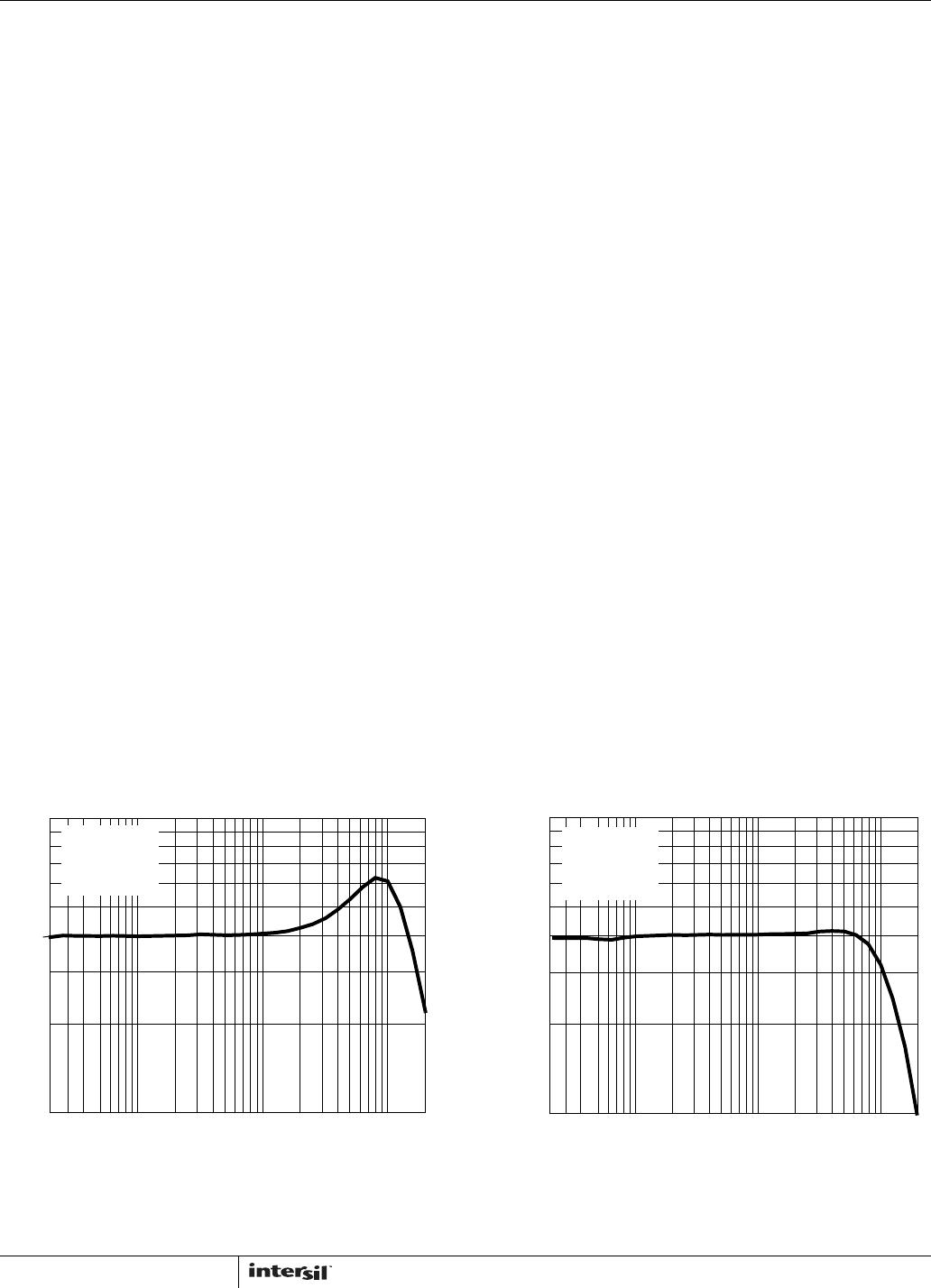
Typical Performance Curves T
A
= +25°C, Unless Otherwise Specified.
FIGURE 1. THD+N vs FREQUENCY FIGURE 2. THD+N vs FREQUENCY
THD+N (%)
FREQUENCY (Hz)
0.1
1.0
0.2
0.3
0.4
0.5
0.6
0.7
0.8
0.9
20 20k50 100 200 500 1k 2k 5k 10k
V
DD
= 5V
BTL
R
L
= 8
P
O
= 800mW
THD+N (%)
FREQUENCY (Hz)
0.1
1.0
0.2
0.3
0.4
0.5
0.6
0.7
0.8
0.9
20 20k50 100 200 500 1k 2k 5k 10k
V
DD
= 3.6V
BTL
R
L
= 8
P
O
= 200mW
ISL54003, ISL54005, ISL54006