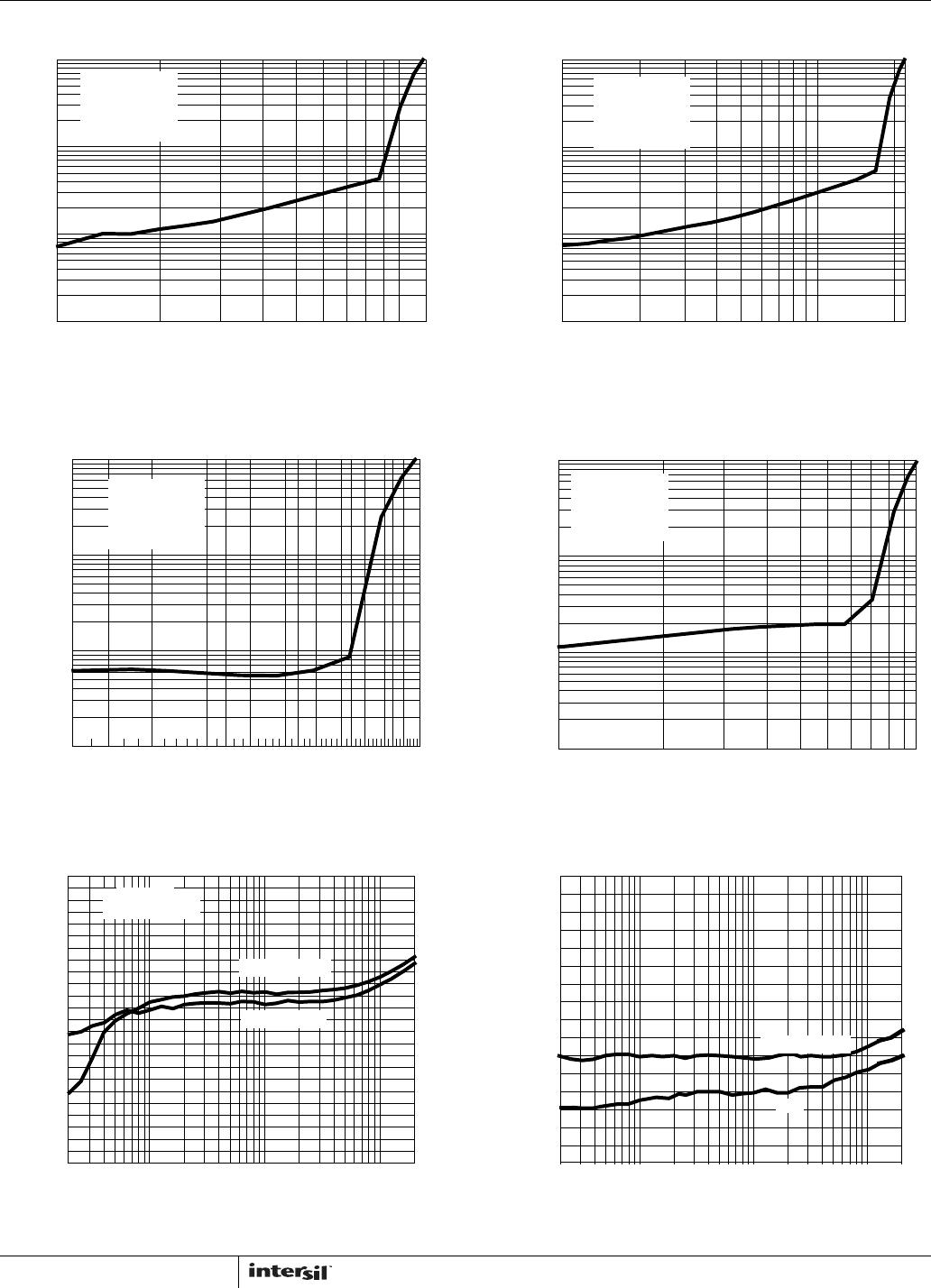
15
All Intersil U.S. products are manufactured, assembled and tested utilizing ISO9001 quality systems.
Intersil Corporation’s quality certifications can be viewed at www.intersil.com/design/quality
Intersil products are sold by description only. Intersil Corporation reserves the right to make changes in circuit design, software and/or specifications at any time without
notice. Accordingly, the reader is cautioned to verify that data sheets are current before placing orders. Information furnished by Intersil is believed to be accurate and
reliable. However, no responsibility is assumed by Intersil or its subsidiaries for its use; nor for any infringements of patents or other rights of third parties which may result
from its use. No license is granted by implication or otherwise under any patent or patent rights of Intersil or its subsidiaries.
For information regarding Intersil Corporation and its products, see www.intersil.com
FN6514.2
October 30, 2007
ISL54003, ISL54005, ISL54006
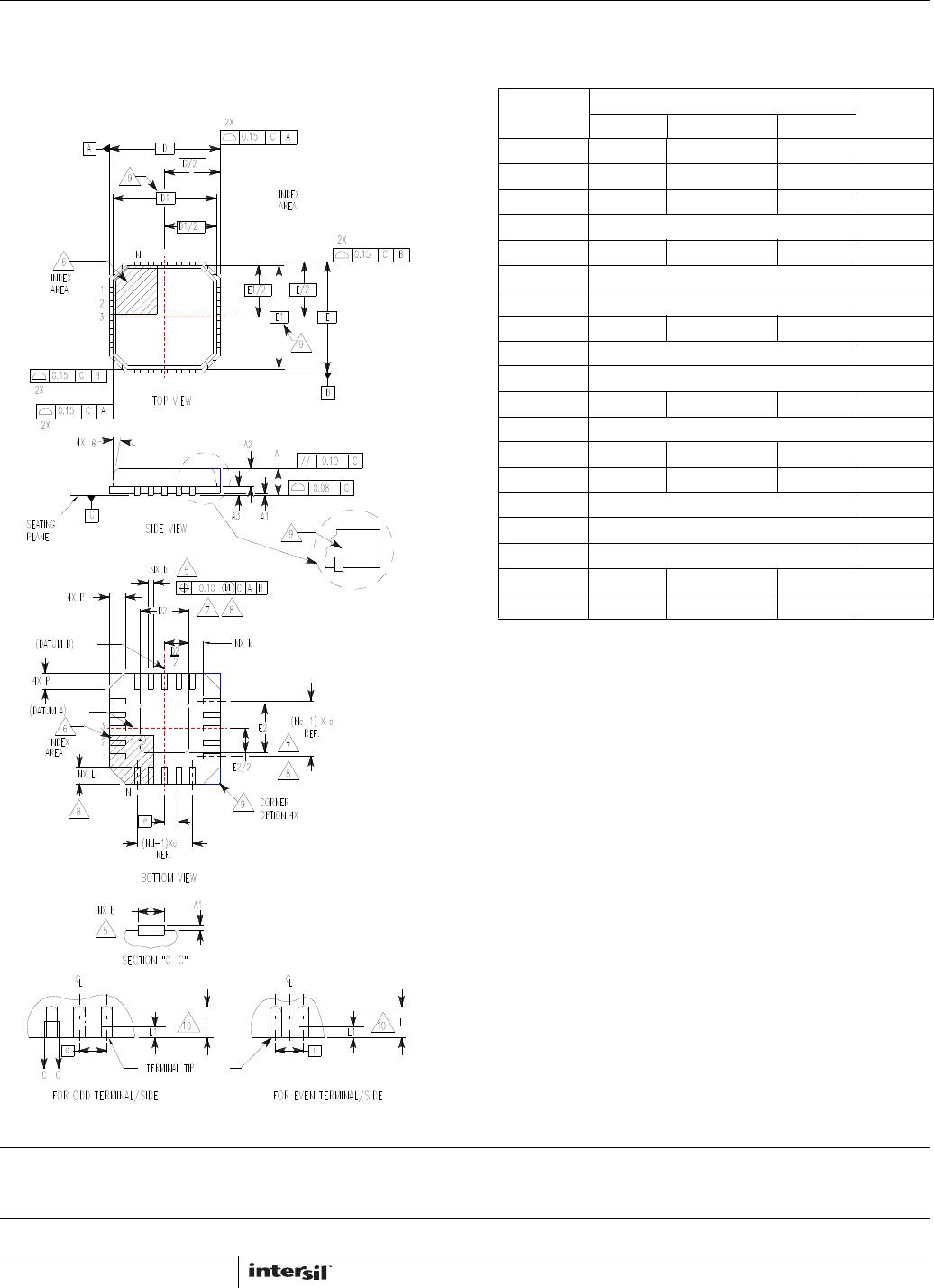
Thin Quad Flat No-Lead Plastic Package
(TQFN)
Thin Micro Lead FramePlastic Package
(TMLFP)
L20.4x4A
20 LEAD QUAD FLAT NO-LEAD PLASTIC PACKAGE
(COMPLIANT TO JEDEC MO-220WGGD-1 ISSUE I)
SYMBOL
MILLIMETERS
NOTESMIN NOMINAL MAX
A 0.70 0.75 0.80 -
A1 - 0.02 0.05 -
A2 - 0.55 0.80 9
A3 0.20 REF 9
b 0.18 0.25 0.30 5, 8
D 4.00 BSC -
D1 3.75 BSC 9
D2 1.95 2.10 2.25 7, 8
E 4.00 BSC -
E1 3.75 BSC 9
E2 1.95 2.10 2.25 7, 8
e 0.50 BSC -
k0.20 - - -
L 0.35 0.60 0.75 8
N202
Nd 5 3
Ne 5 3
P- -0.609
--129
Rev. 0 11/04
NOTES:
1. Dimensioning and tolerancing conform to ASME Y14.5-1994.
2. N is the number of terminals.
3. Nd and Ne refer to the number of terminals on each D and E.
4. All dimensions are in millimeters. Angles are in degrees.
5. Dimension b applies to the metallized terminal and is measured
between 0.15mm and 0.30mm from the terminal tip.
6. The configuration of the pin #1 identifier is optional, but must be
located within the zone indicated. The pin #1 identifier may be
either a mold or mark feature.
7. Dimensions D2 and E2 are for the exposed pads which provide
improved electrical and thermal performance.
8. Nominal dimensions are provided to assist with PCB Land Pattern
Design efforts, see Intersil Technical Brief TB389.
9. Features and dimensions A2, A3, D1, E1, P & are present when
Anvil singulation method is used and not present for saw
singulation.