4
FN6514.2
October 30, 2007
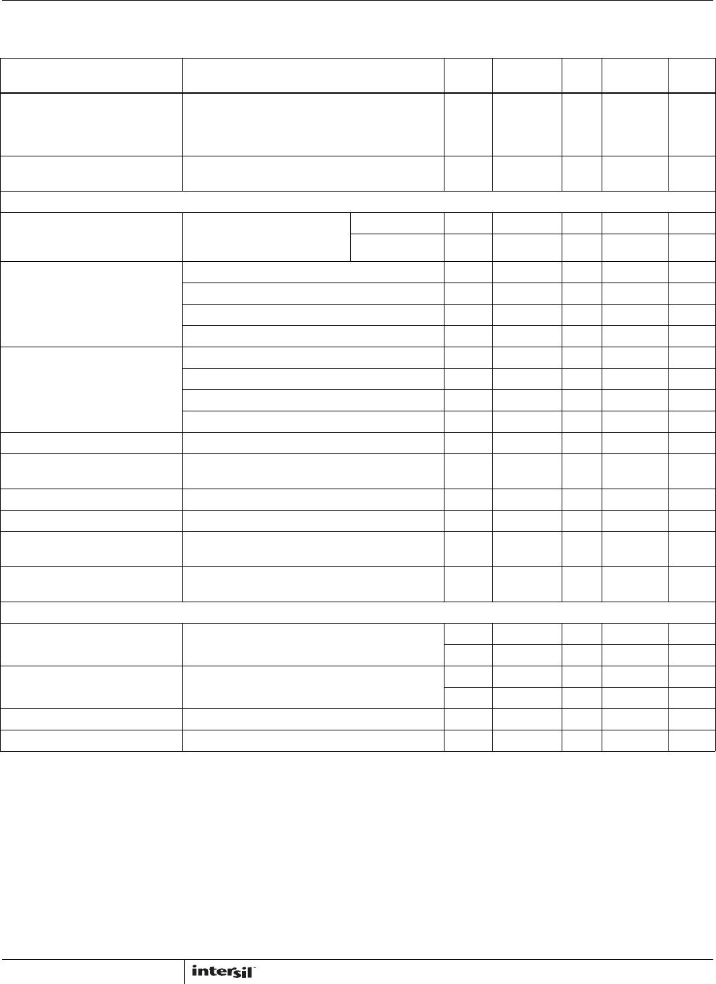
Absolute Maximum Ratings Thermal Information
VDD to GND . . . . . . . . . . . . . . . . . . . . . . . . . . . . . . . . -0.3 to +6.5V
Input Voltages
In_R, In_L, SD, INS, MIX, H_. . . . . . . . . . . . -0.3 to (VDD + 0.3V)
Output Voltages
SPK+, SPK-, Hp_ . . . . . . . . . . . . . . . . . . . . . -0.3 to (VDD + 0.3V)
Continuous Current (VDD, SPK_, Hp_, GND) . . . . . . . . . . . . 750mA
ESD Rating:
Human Body Model . . . . . . . . . . . . . . . . . . . . . . . . . . . . . . . .>2kV
Machine Model . . . . . . . . . . . . . . . . . . . . . . . . . . . . . . . . . . .>200V
Charged Device Model. . . . . . . . . . . . . . . . . . . . . . . . . . . . . .>1kV
Operating Conditions
Temperature Range . . . . . . . . . . . . . . . . . . . . . . . . . .-40°C to +85°C
Thermal Resistance (Typical, Notes 1, 2)
JA
(°C/W)
JC
(°C/W)
20 Ld 4x4 TQFN Package . . . . . . . . . . 45 6.5
Maximum Junction Temperature. . . . . . . . . . . . . . . . . . . . . . . . . +150°C
Maximum Storage Temperature Range . . . . . . . . . . . -65°C to +150°C
Pb-free reflow profile . . . . . . . . . . . . . . . . . . . . . . . . . .see link below
http://www.intersil.com/pbfree/Pb-FreeReflow.asp
CAUTION: Do not operate at or near the maximum ratings listed for extended periods of time. Exposure to such conditions may adversely impact product reliability and
result in failures not covered by warranty.
NOTE:
1.
JA
is measured in free air with the component mounted on a high effective thermal conductivity test board with “direct attach” features.
JC,
the
“case temp” is measured at the center of the exposed metal pad on the package underside. See Tech Brief TB379.
2. For
JC
, the “case temp” location is the center of the exposed metal pad on the package underside.
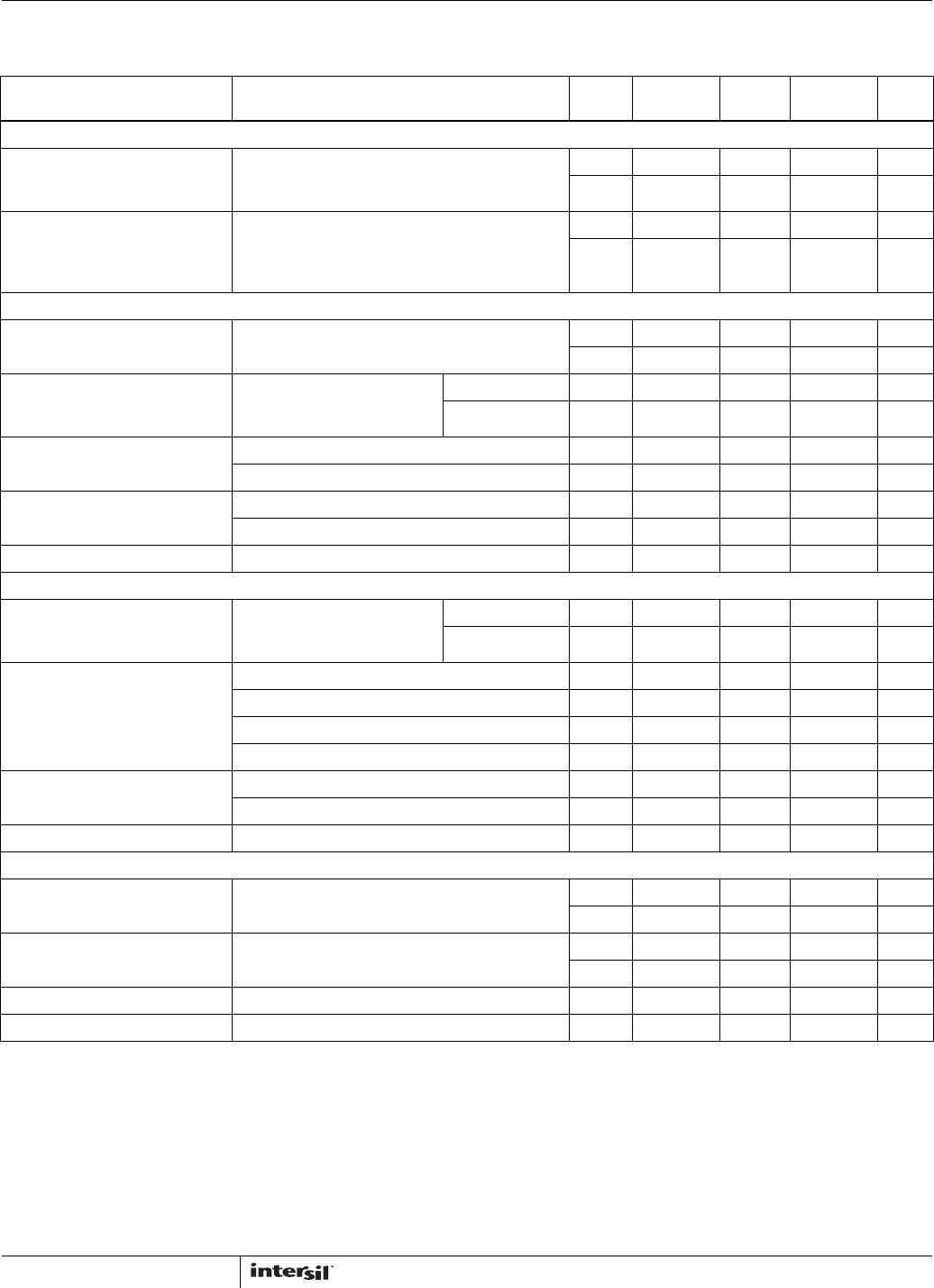
Electrical Specifications - 5V Supply Test Conditions: V
DD
= +5V, GND = 0V, V
INH
= 2.4V, V
INL
= 0.8V, SD = MIX = INS = HD =
V
INL
, C
REF
= 1µF, R
L
is terminated between SPK+ and SPK- for BTL driver and between
Hp_ and GND for SE drivers, Unless Otherwise Specified (Note 3).
PARAMETER TEST CONDITIONS
TEMP
(°C)
MIN
(Notes 4, 5) TYP
MAX
(Notes 4, 5) UNITS
GENERAL
Power Supply Range, V
DD
Full 2.7 - 5.5 V
Quiescent Supply Current, I
DD
HO = V
INL
or V
INH
, HD = V
INL
, INS = V
INL
or V
INH
,
MIX = V
INL
or V
INH
, R
L
= NoneInputs AC coupled
to ground (0.13µF)
25 - 4.6 12 mA
Full - 5.5 - mA
Shutdown Supply Current, I
SD
SD = V
INH
, HO = V
INL
or V
INH
, HD = V
INL
,
INS = V
INL
or V
INH
, MIX = V
INL
or V
INH
, R
L
= 8
BTLand R
L
= 32SEInputs AC coupled to
ground (0.1µF)
25 - 28 50 µA
Full - 31 - µA
Input Resistance, R
IN
INS = 0V or V
DD
25 - 100 - k
Thermal Shutdown, T
SD
INS = MIX = 0V or V
DD
25 - 150 - °C
Thermal Shutdown Hysteresis 25 - 10 - °C
SD to Full Operation, t
SD(ON)
INS = 0V or 5V, MIX = 0V or 5V Full - 1 - ms
BTL AMPLIFIER DRIVER, HD = V
INH,
HO = V
INH,
UNLESS OTHERWISE SPECIFIED
Output Offset Voltage, V
OS
Measured between SPK+ and SPK-, Inputs AC
coupled to ground (0.1µF)
25 - 38 - mV
Full - 49 - mV
Power Supply Rejection Ratio,
PSRR
V
RIPPLE
= 200mV
P-P
, HD =
V
INL
, R
L
= 8nputs AC
coupled to ground (0.1µF)
F
RIPPLE
= 217Hz 25 - 49 - dB
F
RIPPLE
= 1kHz 25 - 47 - dB
Output Power, P
OUT
R
L
= 8, THD+N = 1%, f = 1kHz 25 - 941 - mW
R
L
= 8, THD+N = 10%, f = 1kHz 25 - 1.23 - W
Total Harmonic Distortion + Noise,
THD + N
R
L
= 8P
OUT
= 800mW, f = 1kHz 25 - 0.4 - %
R
L
= 8P
OUT
= 800mW, f = 20Hz to 20kHz 25 - 0.7 - %
Max Output Voltage Swing, V
OUT
R
L
= 8V
SIGNAL
= 5V
P-P
, f = 1kHz 25 7.2 7.7 - V
P-P
Signal to Noise Ratio, SNR R
L
= 8P
OUT
= 900mW, f = 1kHz 25 - 85 - dB
Output Noise, N
OUT
A - Weight filter, BW = 22Hz to 22kHz 25 - 140 - µV
RMS
ISL54003, ISL54005, ISL54006