NBC12429, NBC12429A
http://onsemi.com
10
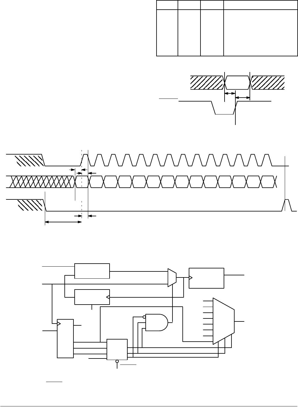
S_CLOCK signal samples the information on the S_DATA
line and loads it into a 14 bit shift register. Note that the
P_LOAD
signal must be HIGH for the serial load operation
to function. The Test register is loaded with the first three
bits, the N register with the next two, and the M register with
the final nine bits of the data stream on the S_DATA input.
For each register, the most significant bit is loaded first (T2,
N1, and M8). A pulse on the S_LOAD pin after the shift
register is fully loaded will transfer the divide values into the
counters. The HIGH to LOW transition on the S_LOAD
input will latch the new divide values into the counters.
Figures 5 and 6 illustrate the timing diagram for both a
parallel and a serial load of the device synthesizer.
M[8:0] and N[1:0] are normally specified once at
powerup through the parallel interface, and then possibly
again through the serial interface. This approach allows the
application to come up at one frequency and then change or
finetune the clock as the ability to control the serial
interface becomes available.
The TEST output provides visibility for one of the several
internal nodes as determined by the T[2:0] bits in the serial
configuration stream. It is not configurable through the
parallel interface. The T2, T1, and T0 control bits are preset
to ‘000’ when P_LOAD
is LOW so that the PECL F
OUT
outputs are as jitterfree as possible. Any active signal on the
TEST output pin will have detrimental affects on the jitter
of the PECL output pair. In normal operations, jitter
specifications are only guaranteed if the TEST output is
static. The serial configuration port can be used to select one
of the alternate functions for this pin.
NBC12429, NBC12429A
http://onsemi.com
11
Table 11. FREQUENCY OPERATING RANGE
VCO Frequency Range for a Crystal Frequency of:
Output Frequency for
F
XTAL
= 16 MHz and for N =
M M[8:0] 10 12 14 16 18 20 B1 B2 B4 B8
160 010100000 200
170 010101010 212.5
180 010110100 202.5 225
190 010111110 213.75 237.5
200 011001000 200 225 250 200 100 50 25
210 011010010 210 236.25 262.5 210 105 52.5 26.25
220 011011100 220 247.5 275 220 110 55 27.5
230 011100110 201.25 230 258.75 287.5 230 115 57.5 28.75
240 011110000 210 240 270 300 240 120 60 30
250 011111010 218.75 250 281.25 312.5 250 125 62.5 31.25
260 100000100 227.5 260 292.5 325 260 130 65 32.5
270 100001110 202.5 236.25 270 303.75 337.5 270 135 67.5 33.75
280 100011000 210 245 280 315 350 280 140 70 35
290 100100010 217.5 253.75 290 326.25 362.5 290 145 72.5 36.25
300 100101100 225 262.5 300 337.5 375 300 150 75 37.5
310 100110110 232.5 271.25 310 348.75 387.5 310 155 77.5 38.75
320 101000000 200 240 280 320 360 400 320 160 80 40
330 101001010 206.25 247.5 288.75 330 371.25 330 165 82.5 41.25
340 101010100 212.5 255 297.5 340 382.5 340 170 85 42.5
350 101011110 218.75 262.5 306.25 350 393.75 350 175 87.5 43.75
360 101101000 225 270 315 360 360 180 90 45
370 101110010 231.25 277.5 323.75 370 370 185 92.5 46.25
380 101111100 237.5 285 332.5 380 380 190 95 47.5
390 110000110 243.75 292.5 341.25 390 390 195 97.5 48.75
400 110010000 250 300 350 400 400 200 100 50
410 110011010 256.25 307.5 358.75
420 110100100 262.5 315 367.5
430 110101110 268.75 322.5 376.25
440 110111000 275 330 385
450 111000010 281.25 337.5 393.75
460 111001100 287.5 345
470 111010110 293.75 352.5
480 111100000 300 360
490 111101010 306.25 367.5
500 111110100 312.5 375
510 111111110 318.75 382.5
NBC12429, NBC12429A
http://onsemi.com
12
Most of the signals available on the TEST output pin are
useful only for performance verification of the device itself.
However, the PLL bypass mode may be of interest at the
board level for functional debug. When T[2:0] is set to 110,
the device is placed in PLL bypass mode. In this mode the
S_CLOCK input is fed directly into the M and N dividers.
The N divider drives the F
OUT
differential pair and the M
counter drives the TEST output pin. In this mode the
S_CLOCK input could be used for low speed board level
functional test or debug. Bypassing the PLL and driving
F
OUT
directly gives the user more control on the test clocks
sent through the clock tree. Figure 7 shows the functional
setup of the PLL bypass mode. Because the S_CLOCK is a
CMOS level the input frequency is limited to 250 MHz or
less. This means the fastest the F
OUT
pin can be toggled via
the S_CLOCK is 250 MHz as the minimum divide ratio of
the N counter is 1. Note that the M counter output on the
TEST output will not be a 50% duty cycle due to the way the
divider is implemented.
T2 T1 T0 TEST (Pin 20)
0
0
0
0
1
1
1
1
0
0
1
1
0
0
1
1
0
1
0
1
0
1
0
1
SHIFT REGISTER OUT
HIGH
F
REF
M COUNTER OUT
F
OUT
LOW
PLL BYPASS
F
OUT
B 4
Figure 5. Parallel Interface Timing Diagram
M[8:0]
N[1:0]
P_LOAD
VALID
t
h
t
s
M, N to P_LOAD
Figure 6. Serial Interface Timing Diagram
S_CLOCK
S_DATA
S_LOAD
Last
Bit
C1 C2 C3 C4 C5 C6 C7 C8 C9 C10 C11 C12
T2 T1 T0 N1 N0 M6 M5 M4 M3 M2 M1 M0
First
Bit
t
s
t
s
t
h
t
h
S_CLOCK to S_LOAD
S_DATA to S_CLOCK
C13 C14
M7M8
Figure 7. Serial Test Clock Block Diagram
FDIV4
MCNT
LOW
F
OUT
MCNT
FREF
HIGH
TEST
MUX
7
0
TEST
F
OUT
(VIA ENABLE GATE)
N B
(1, 2, 4, 8)
0
1
PLL 12430
LATCH
Reset
PLOAD
M COUNTER
SLOAD
T0
T1
T2
VCO_CLK
SHIFT
REG
14BIT
DECODE
SDATA
SCLOCK
MCNT
FREF_EXT
T2=T1=1, T0=0: Test Mode
SCLOCK is selected, MCNT is on TEST output, SCLOCK B N is on F
OUT
pin.
PLOAD
acts as reset for test pin latch. When latch reset, T2 data is shifted out TEST pin.

NBC12429AFN

Mfr. #:
Manufacturer:
ON Semiconductor
Description:
Phase Locked Loops - PLL 3.3V/5V Programmable
Lifecycle:
New from this manufacturer.
Delivery:
DHL FedEx Ups TNT EMS
Payment:
T/T Paypal Visa MoneyGram Western Union