NBC12429, NBC12429A
http://onsemi.com
13
APPLICATIONS INFORMATION
Using the OnBoard Crystal Oscillator
The NBC12429 and NBC12429A feature a fully
integrated onboard crystal oscillator to minimize system
implementation costs. The oscillator is a series resonant,
multivibrator type design as opposed to the more common
parallel resonant oscillator design. The series resonant
design provides better stability and eliminates the need for
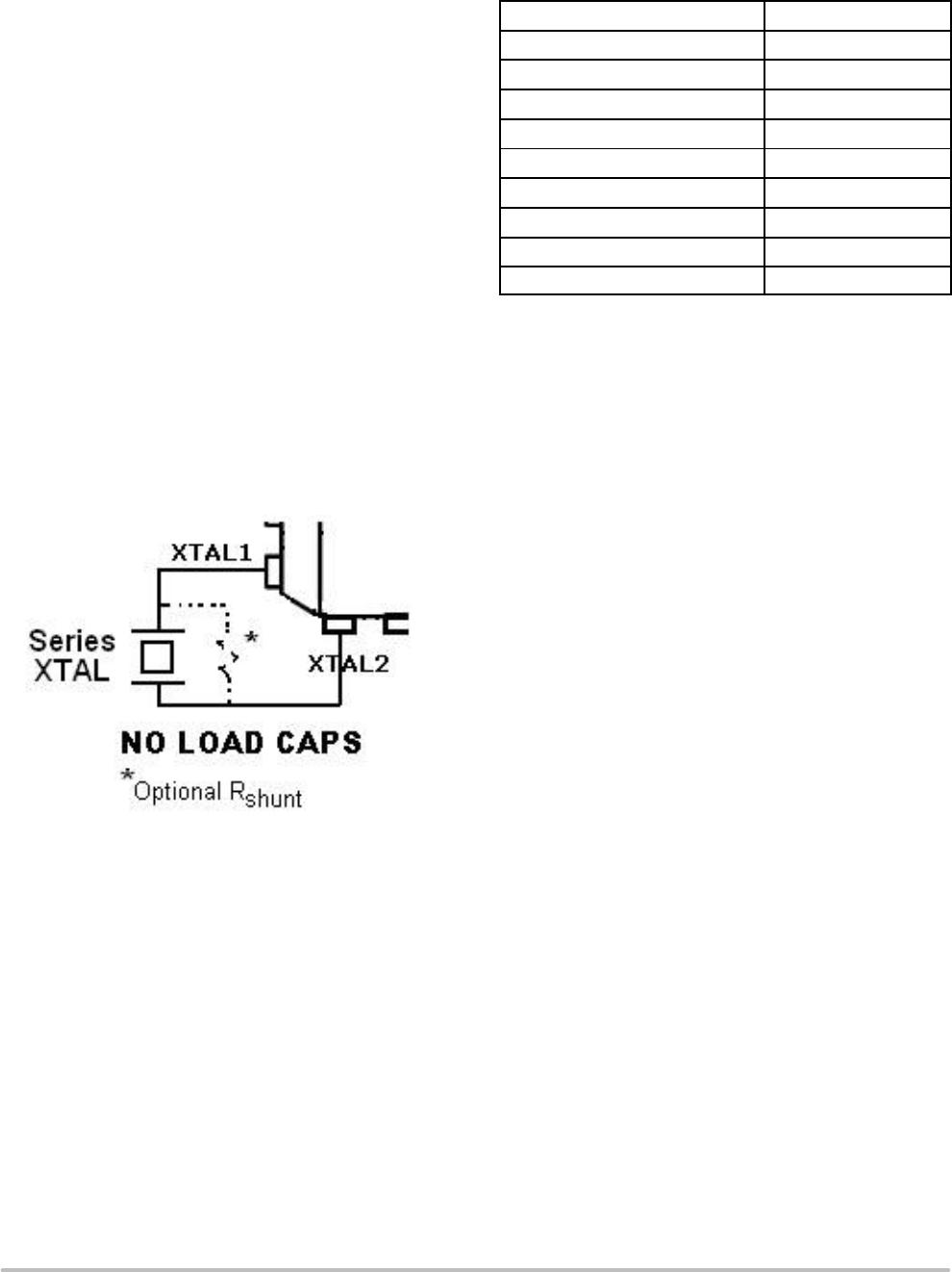
large load capacitors per Figure 8 (do not use cyrstal load
caps). The oscillator is totally self contained so that the only
external component required is the crystal. As the oscillator
is somewhat sensitive to loading on its inputs, the user is
advised to mount the crystal as close to the device as possible
to avoid any board level parasitics. To facilitate colocation,
surface mount crystals are recommended, but not required.
Because the series resonant design is affected by capacitive
loading on the crystal terminals, loading variation
introduced by crystals from different vendors could be a
potential issue. For crystals with a higher shunt capacitance,
it may be required to place a resistance, optional R
shunt
,
across the terminals to suppress the third harmonic.
Although typically not required, it is a good idea to layout
the PCB with the provision of adding this external resistor.
The resistor value will typically be between 500 W and 1 kW.
Figure 8. Crystal Application
The oscillator circuit is a series resonant circuit and thus,
for optimum performance, a series resonant crystal should
be used. Unfortunately, most crystals are characterized in a
parallel resonant mode. Fortunately, there is no physical
difference between a series resonant and a parallel resonant
crystal. The difference is purely in the way the devices are
characterized. As a result, a parallel resonant crystal can be
used with the device with only a minor error in the desired
frequency. A parallel resonant mode crystal used in a series
resonant circuit will exhibit a frequency of oscillation a few
hundred ppm lower than specified (a few hundred ppm
translates to kHz inaccuracies). In a general computer
application, this level of inaccuracy is immaterial. Table 12
below specifies the performance requirements of the
crystals to be used with the device.
Table 12. Crystal Specifications
Parameter Value
Crystal Cut Fundamental AT Cut
Resonance Series Resonance*
Frequency Tolerance ±75 ppm at 25°C
Frequency/Temperature Stability ±150 ppm 0 to 70°C
Operating Range 0 to 70°C
Shunt Capacitance 57 pF
Equivalent Series Resistance (ESR)
50 to 80 W
Correlation Drive Level
100 mW
Aging 5 ppm/Yr (First 3 Years)
*See accompanying text for series versus parallel resonant
discussion.
Power Supply Filtering
The NBC12429 and NBC12429A are mixed
analog/digital products and as such, exhibit some
sensitivities that would not necessarily be seen on a fully
digital product. Analog circuitry is naturally susceptible to
random noise, especially if this noise is seen on the power
supply pins. The NBC12429 and NBC12429A provide
separate power supplies for the digital circuitry (V
CC
) and
the internal PLL (PLL_V
CC
) of the device. The purpose of
this design technique is to try and isolate the high switching
noise of the digital outputs from the relatively sensitive
internal analog PLL. In a controlled environment such as an
evaluation board, this level of isolation is sufficient.
However, in a digital system environment where it is more
difficult to minimize noise on the power supplies, a second
level of isolation may be required. The simplest form of
isolation is a power supply filter on the PLL_V
CC
pin for the
NBC12429 and NBC12429A.
Figure 9 illustrates a typical power supply filter scheme.
The NBC12429 and NBC12429A are most susceptible to
noise with spectral content in the 1 kHz to 1 MHz range.
Therefore, the filter should be designed to target this range.
The key parameter that needs to be met in the final filter
design is the DC voltage drop that will be seen between the
V
CC
supply and the PLL_V
CC
pin of the NBC12429 and
NBC12429A. From the data sheet, the PLL_V
CC
current
(the current sourced through the PLL_V
CC
pin) is typically
23 mA (27 mA maximum). Assuming that a minimum of
2.8 V must be maintained on the PLL_V
CC
pin, very little
DC voltage drop can be tolerated when a 3.3 V V
CC
supply
is used. The resistor shown in Figure 9 must have a
resistance of 10 15 W to meet the voltage drop criteria. The
RC filter pictured will provide a broadband filter with
approximately 100:1 attenuation for noise whose spectral
content is above 20 kHz. As the noise frequency crosses the
series resonant point of an individual capacitor, it’s overall
NBC12429, NBC12429A
http://onsemi.com
14
impedance begins to look inductive and thus increases with
increasing frequency. The parallel capacitor combination
shown ensures that a low impedance path to ground exists
for frequencies well above the bandwidth of the PLL.
Figure 9. Power Supply Filter
PLL_V
CC
V
CC
NBC12429
NBC12429A
0.01 mF
22 mF
L=1000 mH
R=15 W
0.01 mF
3.3 V or
5.0 V
R
S
= 1015 W
3.3 V or
5.0 V
A higher level of attenuation can be achieved by replacing
the resistor with an appropriate valued inductor. Figure 9
shows a 1000 mH choke. This value choke will show a
significant impedance at 10 kHz frequencies and above.
Because of the current draw and the voltage that must be
maintained on the PLL_V
CC
pin, a low DC resistance
inductor is required (less than 15 W). Generally, the
resistor/capacitor filter will be cheaper, easier to implement,
and provide an adequate level of supply filtering.
The NBC12429 and NBC12429A provide
subnanosecond output edge rates and therefore a good
power supply bypassing scheme is a must. Figure 10 shows
a representative board layout for the NBC12429 and
NBC12429A. There exists many different potential board
layouts and the one pictured is but one. The important aspect
of the layout in Figure 10 is the low impedance connections
between V
CC
and GND for the bypass capacitors.
Combining good quality general purpose chip capacitors
with good PCB layout techniques will produce effective
capacitor resonances at frequencies adequate to supply the
instantaneous switching current for the NBC12429 and
NBC12429A outputs. It is imperative that low inductance
chip capacitors are used. It is equally important that the
board layout not introduce any of the inductance saved by
using the leadless capacitors. Thin interconnect traces
between the capacitor and the power plane should be
avoided and multiple large vias should be used to tie the
capacitors to the buried power planes. Fat interconnect and
large vias will help to minimize layout induced inductance
and thus maximize the series resonant point of the bypass
capacitors.
Figure 10. PCB Board Layout (PLCC28)
C2
1
C3
R1
Xtal
C1 C1
R1 = 1015 W
C1 = 0.01 mF
C2 = 22 mF
C3 = 0.1 mF
= V
CC
= GND
= Via
R
shunt
Opt. R
shunt
= 500 1 kW
Note the dotted lines circling the crystal oscillator
connection to the device. The oscillator is a series resonant
circuit and the voltage amplitude across the crystal is
relatively small. It is imperative that no actively switching
signals cross under the crystal as crosstalk energy coupled
to these lines could significantly impact the jitter of the
device. Special attention should be paid to the layout of the
crystal to ensure a stable, jitter free interface between the
crystal and the onboard oscillator. Note the provisions for
placing a resistor across the crystal oscillator terminals as
discussed in the crystal oscillator section of this data sheet.
Although the NBC12429 and NBC12429A have several
design features to minimize the susceptibility to power
supply noise (isolated power and grounds and fully
differential PLL), there still may be applications in which
overall performance is being degraded due to system power
supply noise. The power supply filter and bypass schemes
discussed in this section should be adequate to eliminate
power supply noiserelated problems in most designs.
Jitter Performance
Jitter is a common parameter associated with clock
generation and distribution. Clock jitter can be defined as the
deviation in a clock’s output transition from its ideal
position.
CycletoCycle Jitter is the period variation between
two adjacent cycles over a defined number of observed
cycles. The number of cycles observed is application
NBC12429, NBC12429A
http://onsemi.com
15
dependent but the JEDEC specification is 1000 cycles. Both
PeaktoPeak and RMS statistical values were measured.
Period Jitter is the edge placement deviation observed
over a long period of consecutive cycles compared to the
position of the perfect reference clock’s edge and is specified
by the number of cycles over which the jitter is measured.
The number of cycles used to look for the maximum jitter
varies by application but the JEDEC spec is 10,000 observed
cycles. Both PeaktoPeak and RMS value statistical values
were measured.
Figure 11. CycletoCycle Jitter
T
JITTER(cyclecycle)
= T
1
T
0
T
0
T
1
Table 13 shows the typical Period and CycletoCycle
jitter as a function of the output frequency for selected M and
N values using a 16 MHz crystal. Typical jitter values for
other M and N registers settings may be linearly
interpolated. The general trend is that as the VCO output
frequency is increased, primarily determined by the M
register setting, the output jitter will decrease. Alternate
combinations of M and N register values may produce the
same output frequency but with significantly different jitter
performance.
Table 13. TYPICAL JITTER PERFORMANCE, 3.3 V, 25°C with 16 MHz Crystal Input at Selected M and N Values
JITTER
M Value 200 200 200 200 300 300 300 300 400 400 400 400
N Value 1 2 4 8 1 2 4 8 1 2 4 8
F
OUT
in MHz
CycletoCycle (ps
PP
) 25 106
37.5 67
50 91 44
75 55
100 105 51
150 59
200 98 52
300 58
400 43
CycletoCycle
(ps
RMS
)
25 17
37.5 10
50 13 7
75 9
100 13 8
150 9
200 11 8
300 6
400 6
Period (ps
PP
) 25 106
37.5 56
50 79 35
75 42
100 66 32
150 39

NBC12429AFN

Mfr. #:
Manufacturer:
ON Semiconductor
Description:
Phase Locked Loops - PLL 3.3V/5V Programmable
Lifecycle:
New from this manufacturer.
Delivery:
DHL FedEx Ups TNT EMS
Payment:
T/T Paypal Visa MoneyGram Western Union