NBC12429, NBC12429A
http://onsemi.com
4
The following gives a brief description of the functionality of the NBC12429 and NBC12429A Inputs and Outputs. Unless
explicitly stated, all inputs are CMOS/TTL compatible with either pullup or pulldown resistors. The PECL outputs are capable
of driving two series terminated 50 W transmission lines on the incident edge.
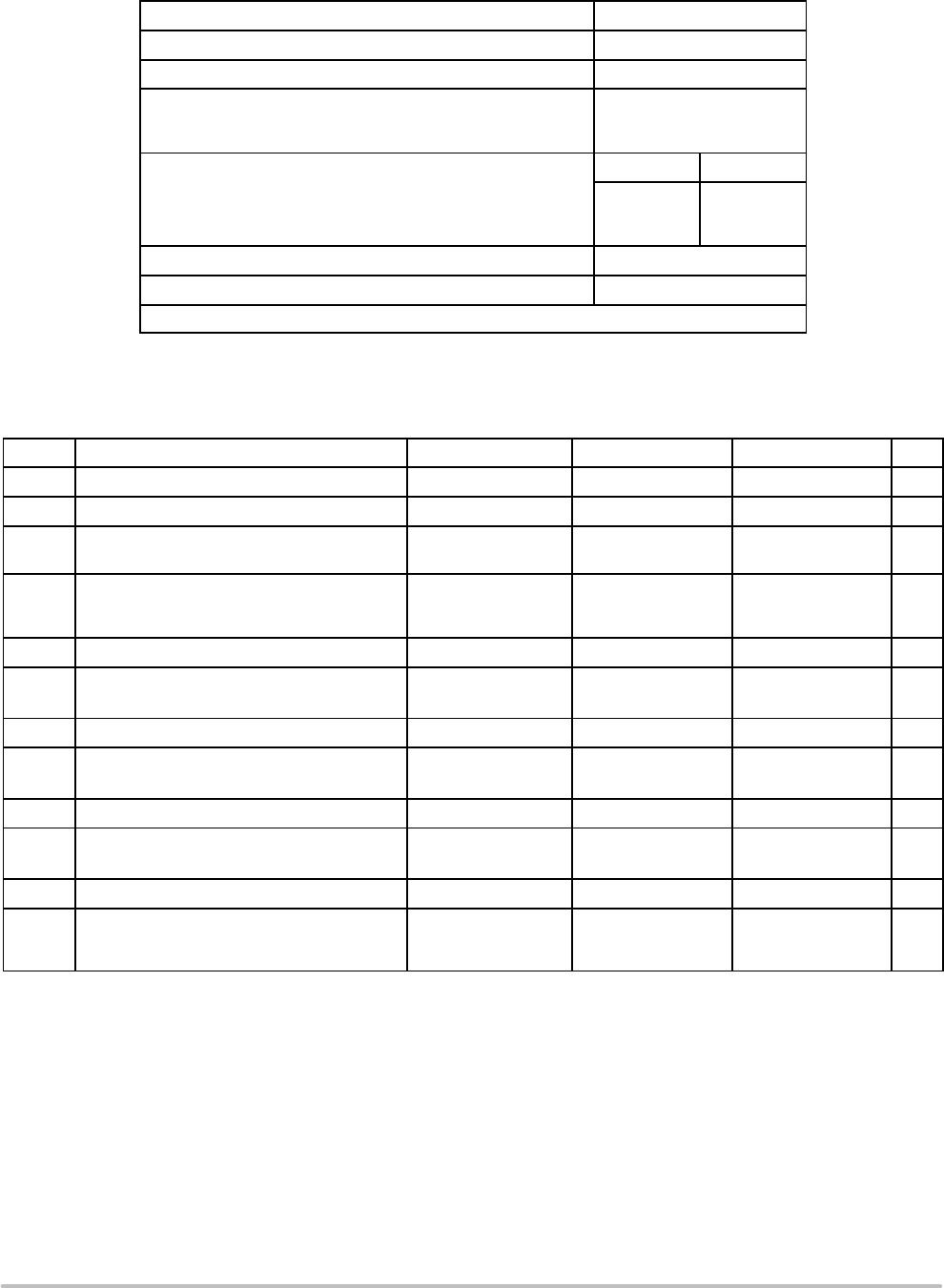
Table 3. PIN FUNCTION DESCRIPTION
Pin Name Function Description
INPUTS
XTAL1, XTAL2
Crystal Inputs These pins form an oscillator when connected to an external seriesresonant
crystal.
S_LOAD* CMOS/TTL Serial Latch Input
(Internal Pulldown Resistor)
This pin loads the configuration latches with the contents of the shift registers. The
latches will be transparent when this signal is HIGH; thus, the data must be stable
on the HIGHtoLOW transition of S_LOAD for proper operation.
S_DATA* CMOS/TTL Serial Data Input
(Internal Pulldown Resistor)
This pin acts as the data input to the serial configuration shift registers.
S_CLOCK* CMOS/TTL Serial Clock Input
(Internal Pulldown Resistor)
This pin serves to clock the serial configuration shift registers. Data from S_DATA
is sampled on the rising edge.
P_LOAD** CMOS/TTL Parallel Latch Input
(Internal Pullup Resistor)
This pin loads the configuration latches with the contents of the parallel inputs.
The latches will be transparent when this signal is LOW; therefore, the parallel
data must be stable on the LOWtoHIGH transition of P_LOAD
for proper opera-
tion.
M[8:0]** CMOS/TTL PLL Loop Divider
Inputs (Internal Pullup Resistor)
These pins are used to configure the PLL loop divider. They are sampled on the
LOWtoHIGH transition of P_LOAD
. M[8] is the MSB, M[0] is the LSB.
N[1:0]** CMOS/TTL Output Divider Inputs
(Internal Pullup Resistor)
These pins are used to configure the output divider modulus. They are sampled
on the LOWtoHIGH transition of P_LOAD
.
OE** CMOS/TTL Output Enable Input
(Internal Pullup Resistor)
Active HIGH Output Enable. The Enable is synchronous to eliminate possibility of
runt pulse generation on the F
OUT
output.
OUTPUTS
F
OUT
, F
OUT
PECL Differential Outputs These differential, positivereferenced ECL signals (PECL) are the outputs of the
synthesizer.
TEST CMOS/TTL Output The function of this output is determined by the serial configuration bits T[2:0].
POWER
V
CC
Positive Supply for the Logic The positive supply for the internal logic and output buffer of the chip, and is con-
nected to +3.3 V or +5.0 V.
PLL_V
CC
Positive Supply for the PLL This is the positive supply for the PLL and is connected to +3.3 V or +5.0 V.
GND Negative Power Supply These pins are the negative supply for the chip and are normally all connected to
ground.
Exposed Pad for QFN32 only The Exposed Pad (EP) on the QFN32 package bottom is thermally connected to
the die for improved heat transfer out of package. The exposed pad must be at-
tached to a heatsinking conduit. The pad is electrically connected to GND.
* When left Open, these inputs will default LOW.
** When left Open, these inputs will default HIGH.
NBC12429, NBC12429A
http://onsemi.com
5
Table 4. ATTRIBUTES
Characteristics Value
Internal Input Pulldown Resistor
75 kW
Internal Input Pullup Resistor
37.5 kW
ESD Protection Human Body Model
Machine Model
Charged Device Model
> 2 kV
> 150 V
> 1 kV
Moisture Sensitivity (Note 1) Pb Pkg PbFree Pkg
PLCC
LQFP
QFN
Level 1
Level 2
Level 1
Level 3
Level 2
Level 1
Flammability Rating Oxygen Index: 28 to 34 UL 94 V0 @ 0.125 in
Transistor Count 2035
Meets or exceeds JEDEC Spec EIA/JESD78 IC Latchup Test
1. For additional information, see Application Note AND8003/D.
Table 5. MAXIMUM RATINGS
Symbol Parameter Condition 1 Condition 2 Rating Unit
V
CC
Positive Supply GND = 0 V 6 V
V
I
Input Voltage GND = 0 V V
I
V
CC
6 V
I
out
Output Current Continuous
Surge
50
100
mA
mA
T
A
Operating Temperature Range
NBC12429
NBC12429A
0 to 70
40 to +85
°C
T
stg
Storage Temperature Range 65 to +150 °C
q
JA
Thermal Resistance (JunctiontoAmbient) 0 lfpm
500 lfpm
PLCC28
PLCC28
63.5
43.5
°C/W
°C/W
q
JC
Thermal Resistance (JunctiontoCase) Standard Board PLCC28 22 to 26 °C/W
q
JA
Thermal Resistance (JunctiontoAmbient) 0 lfpm
500 lfpm
LQFP32
LQFP32
80
55
°C/W
°C/W
q
JC
Thermal Resistance (JunctiontoCase) Standard Board LQFP32 12 to 17 °C/W
q
JA
Thermal Resistance (JunctiontoAmbient) 0 lfpm
500 lfpm
QFN32
QFN32
31
27
°C/W
°C/W
q
JC
Thermal Resistance (JunctiontoCase) 2S2P QFN32 12 °C/W
T
sol
Wave Solder
Pb
PbFree
<3 sec @ 248°C
<3 sec @ 260°C
265
265
°C
Stresses exceeding Maximum Ratings may damage the device. Maximum Ratings are stress ratings only. Functional operation above the
Recommended Operating Conditions is not implied. Extended exposure to stresses above the Recommended Operating Conditions may affect
device reliability.
NBC12429, NBC12429A
http://onsemi.com
6
Table 6. DC CHARACTERISTICS (V
CC
= 3.3 V ± 5%; T
A
= 0°C to 70°C (NBC12429), T
A
= 40°C to 85°C (NBC12429A))
Symbol
Characteristic Condition Min Typ Max Unit
V
IH
LVCMOS/
LVTTL
Input HIGH Voltage V
CC
= 3.3 V 2.0 V
V
IL
LVCMOS/
LVTTL
Input LOW Voltage V
CC
= 3.3 V 0.8 V
I
IN
Input Current 1.0 mA
V
OH
Output HIGH Voltage
TEST
I
OH
= 0.8 mA 2.5 V
V
OL
Output LOW Voltage
TEST
I
OL
= 0.8 mA 0.4 V
V
OH
PECL
Output HIGH Voltage F
OUT
F
OUT
V
CC
= 3.3 V
(Notes 2, 3)
2.155 2.405 V
V
OL
PECL
Output LOW Voltage F
OUT
F
OUT
V
CC
= 3.3 V
(Notes 2, 3)
1.355 1.605 V
I
CC
Power Supply Current V
CC
PLL_V
CC
48
18
58
22
70
26
mA
mA
NOTE: Device will meet the specifications after thermal equilibrium has been established when mounted in a test socket or printed circuit
board with maintained transverse airflow greater than 500 lfpm. Electrical parameters are guaranteed only over the declared
operating temperature range. Functional operation of the device exceeding these conditions is not implied. Device specification limit
values are applied individually under normal operating conditions and not valid simultaneously.
2. F
OUT
/F
OUT
output levels will vary 1:1 with V
CC
variation.
3. F
OUT
/F
OUT
outputs are terminated through a 50 W resistor to V
CC
2.0 V.
Table 7. DC CHARACTERISTICS (V
CC
= 5.0 V ± 5%; T
A
= 0°C to 70°C (NBC12429), T
A
= 40°C to 85°C (NBC12429A))
Symbol Characteristic Condition Min Typ Max Unit
V
IH
CMOS/
TTL
Input HIGH Voltage V
CC
= 5.0 V 2.0 V
V
IL
CMOS/
TTL
Input LOW Voltage V
CC
= 5.0 V 0.8 V
I
IN
Input Current 1.0 mA
V
OH
Output HIGH Voltage TEST I
OH
= 0.8 mA 2.5 V
V
OL
Output LOW Voltage TEST I
OL
= 0.8 mA 0.4 V
V
OH
PECL
Output HIGH Voltage F
OUT
F
OUT
V
CC
= 5.0 V
(Notes 4, 5)
3.855 4.105 V
V
OL
PECL
Output LOW Voltage F
OUT
F
OUT
V
CC
= 5.0 V
(Notes 4, 5)
3.055 3.305 V
I
CC
Power Supply Current V
CC
PLL_V
CC
50
19
60
23
75
27
mA
mA
NOTE: Device will meet the specifications after thermal equilibrium has been established when mounted in a test socket or printed circuit
board with maintained transverse airflow greater than 500 lfpm. Electrical parameters are guaranteed only over the declared
operating temperature range. Functional operation of the device exceeding these conditions is not implied. Device specification limit
values are applied individually under normal operating conditions and not valid simultaneously.
4. F
OUT
/F
OUT
output levels will vary 1:1 with V
CC
variation.
5. F
OUT
/F
OUT
outputs are terminated through a 50 W resistor to V
CC
2.0 V.

NBC12429AFN

Mfr. #:
Manufacturer:
ON Semiconductor
Description:
Phase Locked Loops - PLL 3.3V/5V Programmable
Lifecycle:
New from this manufacturer.
Delivery:
DHL FedEx Ups TNT EMS
Payment:
T/T Paypal Visa MoneyGram Western Union