NBC12429, NBC12429A
http://onsemi.com
7
Table 8. AC CHARACTERISTICS (V
CC
= 3.125 V to 5.25 V; T
A
= 0°C to 70°C (NBC12429), T
A
= 40°C to 85°C (NBC12429A))
(Note 6)
Symbol
Characteristic Condition Min Max Unit
F
MAXI
Maximum Input Frequency S_CLOCK
Xtal Oscillator
(Note 7)
10
10
20
MHz
F
MAXO
Maximum Output Frequency VCO (Internal)
F
OUT
200
25
400
400
MHz
t
jitter(pd)
Period Jitter @ 3.3 V
10000 WFMS
(See Table 13 for Typical Values)
25 MHz < f
OUT
< 100 MHz, M = 200
25 MHz < f
OUT
< 100 MHz, M = 300
25 MHz < f
OUT
< 100 MHz, M = 400
100 MHz < f
OUT
< 400 MHz, M = 200
100 MHz < f
OUT
< 400 MHz, M = 300
100 MHz < f
OUT
< 400 MHz, M = 400
25
9.0
6.0
9.0
5.0
4.0
ps
RMS
25 MHz < f
OUT
< 100 MHz, M = 200
25 MHz < f
OUT
< 100 MHz, M = 300
25 MHz < f
OUT
< 100 MHz, M = 400
100 MHz < f
OUT
< 400 MHz, M = 200
100 MHz < f
OUT
< 400 MHz, M = 300
100 MHz < f
OUT
< 400 MHz, M = 400
146
71
53
125
60
54
ps
PP
Period Jitter @ 5.0 V
10000 WFMS
(See Table 13 for Typical Values)
25 MHz < f
OUT
< 100 MHz, M = 200
25 MHz < f
OUT
< 100 MHz, M = 300
25 MHz < f
OUT
< 100 MHz, M = 400
100 MHz < f
OUT
< 400 MHz, M = 200
100 MHz < f
OUT
< 400 MHz, M = 300
100 MHz < f
OUT
< 400 MHz, M = 400
25
9.0
6.0
10
6.0
5.0
ps
RMS
25 MHz < f
OUT
< 100 MHz, M = 200
25 MHz < f
OUT
< 100 MHz, M = 300
25 MHz < f
OUT
< 100 MHz, M = 400
100 MHz < f
OUT
< 400 MHz, M = 200
100 MHz < f
OUT
< 400 MHz, M = 300
100 MHz < f
OUT
< 400 MHz, M = 400
168
69
57
133
49
108
ps
PP
t
jitter(cyccyc)
CycletoCycle @ 3.3 V
1000 WFMS
(See Table 13 for Typical Values)
25 MHz < f
OUT
< 100 MHz, M = 200
25 MHz < f
OUT
< 100 MHz, M = 300
25 MHz < f
OUT
< 100 MHz, M = 400
100 MHz < f
OUT
< 400 MHz, M = 200
100 MHz < f
OUT
< 400 MHz, M = 300
100 MHz < f
OUT
< 400 MHz, M = 400
20
11
8.0
17
10
9.0
ps
RMS
25 MHz < f
OUT
< 100 MHz, M = 200
25 MHz < f
OUT
< 100 MHz, M = 300
25 MHz < f
OUT
< 100 MHz, M = 400
100 MHz < f
OUT
< 400 MHz, M = 200
100 MHz < f
OUT
< 400 MHz, M = 300
100 MHz < f
OUT
< 400 MHz, M = 400
150
105
77
208
94
89
ps
PP
CycletoCycle @ 5.0 V
1000 WFMS
(See Table 13 for Typical Values)
25 MHz < f
OUT
< 100 MHz, M = 200
25 MHz < f
OUT
< 100 MHz, M = 300
25 MHz < f
OUT
< 100 MHz, M = 400
100 MHz < f
OUT
< 400 MHz, M = 200
100 MHz < f
OUT
< 400 MHz, M = 300
100 MHz < f
OUT
< 400 MHz, M = 400
25
12
8.0
18
11
10
ps
RMS
25 MHz < f
OUT
< 100 MHz, M = 200
25 MHz < f
OUT
< 100 MHz, M = 300
25 MHz < f
OUT
< 100 MHz, M = 400
100 MHz < f
OUT
< 400 MHz, M = 200
100 MHz < f
OUT
< 400 MHz, M = 300
100 MHz < f
OUT
< 400 MHz, M = 400
192
131
76
164
128
186
ps
PP
t
LOCK
Maximum PLL Lock Time 10 ms
NOTE: Device will meet the specifications after thermal equilibrium has been established when mounted in a test socket or printed circuit
board with maintained transverse airflow greater than 500 lfpm. Electrical parameters are guaranteed only over the declared
operating temperature range. Functional operation of the device exceeding these conditions is not implied. Device specification
limit values are applied individually under normal operating conditions and not valid simultaneously.
6. F
OUT
/F
OUT
outputs are terminated through a 50 W resistor to V
CC
2.0 V.
7. 10 MHz is the maximum frequency to load the feedback divide registers. S_CLOCK can be switched at higher frequencies when used
as a test clock in TEST_MODE 6.
NBC12429, NBC12429A
http://onsemi.com
8
Table 8. AC CHARACTERISTICS (V
CC
= 3.125 V to 5.25 V; T
A
= 0°C to 70°C (NBC12429), T
A
= 40°C to 85°C (NBC12429A))
(Note 6)
Symbol UnitMaxMinConditionCharacteristic
t
s
Setup Time S_DATA to S_CLOCK
S_CLOCK to S_LOAD
M, N to P_LOAD
20
20
20
ns
t
h
Hold Time S_DATA to S_CLOCK
M, N to P_LOAD
20
20
ns
t
pwMIN
Minimum Pulse Width S_LOAD
P_LOAD
50
50
ns
DCO Output Duty Cycle 47.5 52.5 %
t
r
, t
f
Output Rise/Fall F
OUT
20%80% 175 425 ps
NOTE: Device will meet the specifications after thermal equilibrium has been established when mounted in a test socket or printed circuit
board with maintained transverse airflow greater than 500 lfpm. Electrical parameters are guaranteed only over the declared
operating temperature range. Functional operation of the device exceeding these conditions is not implied. Device specification
limit values are applied individually under normal operating conditions and not valid simultaneously.
6. F
OUT
/F
OUT
outputs are terminated through a 50 W resistor to V
CC
2.0 V.
7. 10 MHz is the maximum frequency to load the feedback divide registers. S_CLOCK can be switched at higher frequencies when used
as a test clock in TEST_MODE 6.
FUNCTIONAL DESCRIPTION
The internal oscillator uses the external quartz crystal as
the basis of its frequency reference. The output of the
reference oscillator is divided by 16 before being sent to the
phase detector. With a 16 MHz crystal, this provides a
reference frequency of 1 MHz. Although this data sheet
illustrates functionality only for a 16 MHz crystal, Table 9,
any crystal in the 10 MHz 20 MHz range can be used,
Table 11.
The VCO within the PLL operates over a range of 200 to
400 MHz. Its output is scaled by a divider that is configured
by either the serial or parallel interfaces. The output of this
loop divider is also applied to the phase detector.
The phase detector and the loop filter force the VCO
output frequency to be M times the reference frequency by
adjusting the VCO control voltage. Note that for some
values of M (either too high or too low), the PLL will not
achieve loop lock.
The output of the VCO is also passed through an output
divider before being sent to the PECL output driver. This
output divider (N divider) is configured through either the
serial or the parallel interfaces and can provide one of four
division ratios (1, 2, 4, or 8). This divider extends the
performance of the part while providing a 50% duty cycle.
The output driver is driven differentially from the output
divider and is capable of driving a pair of transmission lines
terminated into 50 W to V
CC
2.0 V. The positive reference
for the output driver and the internal logic is separated from
the power supply for the PLL to minimize noise induced
jitter.
The configuration logic has two sections: serial and
parallel. The parallel interface uses the values at the M[8:0]
and N[1:0] inputs to configure the internal counters.
Normally upon system reset, the P_LOAD
input is held
LOW until sometime after power becomes valid. On the
LOWtoHIGH transition of P_LOAD
, the parallel inputs
are captured. The parallel interface has priority over the
serial interface. Internal pullup resistors are provided on the
M[8:0] and N[1:0] inputs to reduce component count in the
application of the chip.
The serial interface logic is implemented with a fourteen
bit shift register scheme. The register shifts once per rising
edge of the S_CLOCK input. The serial input S_DATA must
meet setup and hold timing as specified in the AC
Characteristics section of this document. With P_LOAD
held high, the configuration latches will capture the value of
the shift register on the HIGHtoLOW edge of the
S_LOAD input. See the programming section for more
information.
The TEST output reflects various internal node values and
is controlled by the T[2:0] bits in the serial data stream. See
the programming section for more information.
NBC12429, NBC12429A
http://onsemi.com
9
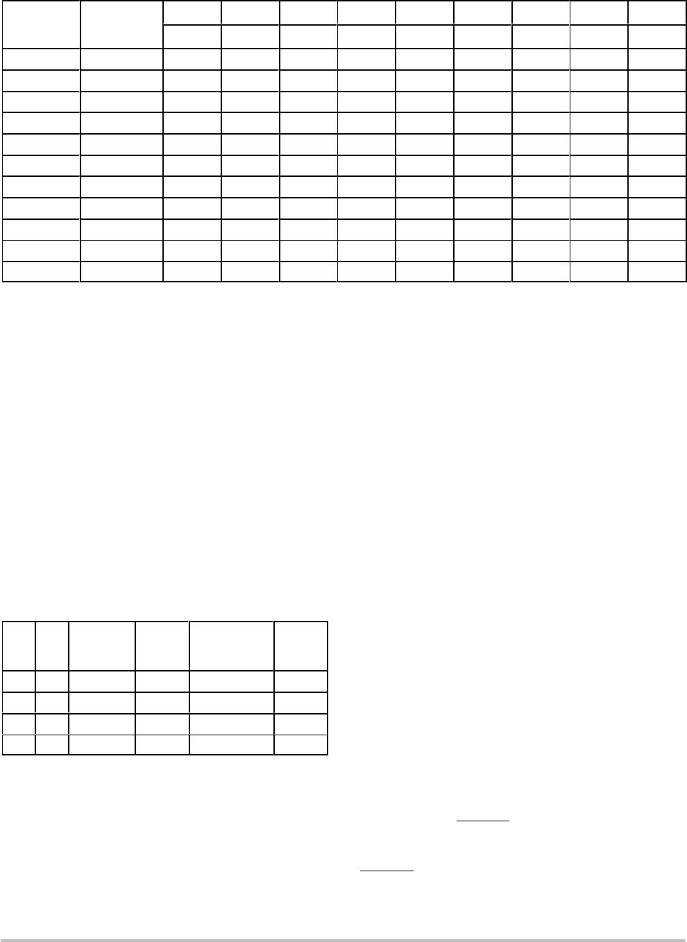
Table 9. PROGRAMMING VCO FREQUENCY FUNCTION TABLE WITH 16 MHZ CRYSTAL
VCO
Frequency
(MHz)
M
Count
Divisor
256 128 64 32 16 8 4 2 1
M8 M7 M6 M5 M4 M3 M2 M1 M0
200 200 0 1 1 0 0 1 0 0 0
201 201 0 1 1 0 0 1 0 0 1
202 202 0 1 1 0 0 1 0 1 0
203 203 0 1 1 0 0 1 0 1 1
397 397 1 1 0 0 0 1 1 0 1
398 398 1 1 0 0 0 1 1 1 0
399 399 1 1 0 0 0 1 1 1 1
400 400 1 1 0 0 1 0 0 0 0
PROGRAMMING INTERFACE
Programming the NBC12429 and NBC12429A is
accomplished by properly configuring the internal dividers
to produce the desired frequency at the outputs. The output
frequency can by represented by this formula:
FOUT + (F
XTAL
B 16) M B N
(eq. 1)
where F
XTAL
is the crystal frequency, M is the loop divider
modulus, and N is the output divider modulus. Note that it
is possible to select values of M such that the PLL is unable
to achieve loop lock. To avoid this, always make sure that M
is selected to be 200 M 400 for a 16 MHz input reference.
Assuming that a 16 MHz reference frequency is used the
above equation reduces to:
F
OUT
+ M B N
(eq. 2)
Substituting the four values for N (1, 2, 4, 8) yields:
Table 10. Programmable Output Divider Function
N1 N0 N Divider F
OUT
Output
Frequency
Range (MHz)*
F
OUT
Step
0 0 B1 M 200400 1 MHz
0 1 B2 M B 2 100200 500 kHz
1 0 B4 M B 4 50100 250 kHz
1 1 B8 M B 8 2550 125 kHz
*For crystal frequency of 16 MHz.
The user can identify the proper M and N values for the
desired frequency from the above equations. The four output
frequency ranges established by N are
200 MHz 400 MHz, 100 MHz 200 MHz,
50 MHz 100 MHz and 25 MHz 50 MHz, respectively.
From these ranges, the user will establish the value of N
required. The value of M can then be calculated based on
Equation 1. For example, if an output frequency of
131 MHz was desired, the following steps would be taken to
identify the appropriate M and N values. 131 MHz falls
within the frequency range set by an N value of 2; thus, N
[1:0] = 01. For N = 2, F
OUT
= M ÷ 2 and M = 2 x F
OUT
.
Therefore,
M + 131 2 + 262, soM[8 : 0] + 100000110.
Following this same procedure, a user can generate any
whole frequency desired between 25 and 400 MHz. Note
that for N > 2, fractional values of F
OUT
can be realized. The
size of the programmable frequency steps (and thus, the
indicator of the fractional output frequencies achievable)
will be equal to F
XTAL
÷ 16 ÷ N.
For input reference frequencies other than 16 MHz, see
Table 11, which shows the usable VCO frequency and
M divider range.
The input frequency and the selection of the feedback
divider M is limited by the VCO frequency range and
F
XTAL
. M must be configured to match the VCO frequency
range of 200 MHz to 400 MHz in order to achieve stable
PLL operation.
M
min
+ f
VCOmin
B (f
XTAL
B 16) and
(eq. 3)
M
max
+ f
VCOmax
B (f
XTAL
B 16)
(eq. 4)
The value for M falls within the constraints set for PLL
stability. If the value for M fell outside of the valid range, a
different N value would be selected to move M in the
appropriate direction.
The M and N counters can be loaded either through a
parallel or serial interface. The parallel interface is
controlled via the P_LOAD
signal such that a LOW to HIGH
transition will latch the information present on the M[8:0]
and N[1:0] inputs into the M and N counters. When the
P_LOAD
signal is LOW, the input latches will be
transparent and any changes on the M[8:0] and N[1:0] inputs
will affect the F
OUT
output pair. To use the serial port, the

NBC12429AFN

Mfr. #:
Manufacturer:
ON Semiconductor
Description:
Phase Locked Loops - PLL 3.3V/5V Programmable
Lifecycle:
New from this manufacturer.
Delivery:
DHL FedEx Ups TNT EMS
Payment:
T/T Paypal Visa MoneyGram Western Union