Low Noise, Low Drift
Single-Supply Operational Amplifiers
OP113/OP213/OP413
Rev. F
Information furnished by Analog Devices is believed to be accurate and reliable. However, no
responsibility is assumed by Analog Devices for its use, nor for any infringements of patents or other
rights of third parties that may result from its use. Specifications subject to change without notice. No
license is granted by implication or otherwise under any patent or patent rights of Analog Devices.
Trademarks and registered trademarks are the property of their respective owners.
One Technology Way, P.O. Box 9106, Norwood, MA 02062-9106, U.S.A.
Tel: 781.329.4700 www.analog.com
Fax: 781.461.3113 ©1993–2007 Analog Devices, Inc. All rights reserved.
FEATURES
Single- or dual-supply operation
Low noise: 4.7 nV/√Hz @ 1 kHz
Wide bandwidth: 3.4 MHz
Low offset voltage: 100 μV
Very low drift: 0.2 μV/°C
Unity gain stable
No phase reversal
APPLICATIONS
Digital scales
Multimedia
Strain gages
Battery-powered instrumentation
Temperature transducer amplifier
GENERAL DESCRIPTION
The OPx13 family of single-supply operational amplifiers
features both low noise and drift. It has been designed for
systems with internal calibration. Often these processor-based
systems are capable of calibrating corrections for offset and
gain, but they cannot correct for temperature drifts and noise.
Optimized for these parameters, the OPx13 family can be used
to take advantage of superior analog performance combined
with digital correction. Many systems using internal calibration
operate from unipolar supplies, usually either 5 V or 12 V. The
OPx13 family is designed to operate from single supplies from
4 V to 36 V and to maintain its low noise and precision
performance.
The OPx13 family is unity gain stable and has a typical gain
bandwidth product of 3.4 MHz. Slew rate is in excess of 1 V/s.
Noise density is a very low 4.7 nV/√Hz, and noise in the 0.1 Hz
to 10 Hz band is 120 nV p-p. Input offset voltage is guaranteed
and offset drift is guaranteed to be less than 0.8 V/°C. Input
common-mode range includes the negative supply and to
within 1 V of the positive supply over the full supply range.
Phase reversal protection is designed into the OPx13 family for
cases where input voltage range is exceeded. Output voltage
swings also include the negative supply and go to within 1 V of
the positive rail. The output is capable of sinking and sourcing
current throughout its range and is specified with 600 loads.
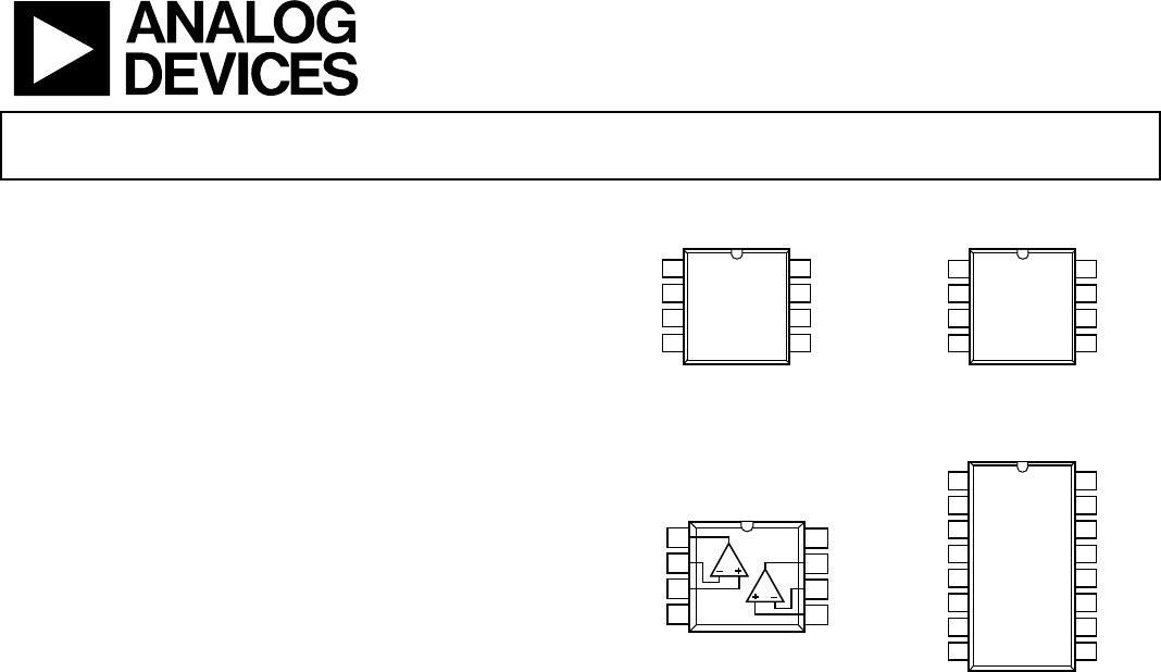
PIN CONFIGURATIONS
NULL
1
–IN A
2
+IN A
3
V–
4
NC
8
V+
7
OUT A
6
NULL
5
OP113
TOP VIEW
(Not to Scale)
NC = NO CONNECT
00286-001
OUT A
1
–IN A
2
+IN A
3
V–
4
V+
8
OUT B
7
–IN B
6
+IN B
5
OP213
TOP VIEW
(Not to Scale)
0286-002
Figure 1. 8-Lead Narrow-Body
SOIC_N
Figure 2. 8-Lead Narrow-Body
SOIC_N
OUT A
1
–IN A
2
+IN A
3
V–
4
V+
8
OUT B
7
–IN B
6
+IN B
5
OP213
-
OUT A
1
–IN A
2
+IN A
3
V+
4
OUT D
16
–IN D
15
+IN D
14
V–
13
+IN B
5
+IN C
12
–IN B
6
–IN C
11
OUT B
7
OUT C
10
NC
8
NC
9
NC = NO CONNECT
OP413
TOP VIEW
(Not to Scale)
00286-004
Figure 3. 8-Lead PDIP Figure 4. 16-Lead Wide-Body
SOIC_W
Digital scales and other strain gage applications benefit from
the very low noise and low drift of the OPx13 family. Other
applications include use as a buffer or amplifier for both analog-
to-digital (ADC) and digital-to-analog (DAC) sigma-delta
converters. Often these converters have high resolutions
requiring the lowest noise amplifier to utilize their full
potential. Many of these converters operate in either single-
supply or low-supply voltage systems, and attaining the greater
signal swing possible increases system performance.
The OPx13 family is specified for single 5 V and dual ±15 V
operation over the XIND—extended industrial temperature
range (–40°C to +85°C). They are available in PDIP and SOIC
surface-mount packages.