OP113/OP213/OP413
Rev. F | Page 13 of 24
APPLICATIONS
The OP113, OP213, and OP413 form a new family of high
performance amplifiers that feature precision performance in
standard dual-supply configurations and, more importantly,
maintain precision performance when a single power supply is
used. In addition to accurate dc specifications, it is the lowest
noise single-supply amplifier available with only 4.7 nV/√Hz
typical noise density.
Single-supply applications have special requirements due to the
generally reduced dynamic range of the output signal. Single-
supply applications are often operated at voltages of 5 V or 12 V,
compared to dual-supply applications with supplies of ±12 V or
±15 V. This results in reduced output swings. Where a dual-
supply application may often have 20 V of signal output swing,
single-supply applications are limited to, at most, the supply
range and, more commonly, several volts below the supply.
In order to attain the greatest swing, the single-supply output
stage must swing closer to the supply rails than in dual-supply
applications.
The OPx13 family has a new patented output stage that allows
the output to swing closer to ground, or the negative supply,
than previous bipolar output stages. Previous op amps had
outputs that could swing to within about 10 mV of the negative
supply in single-supply applications. However, the OPx13
family combines both a bipolar and a CMOS device in the output
stage, enabling it to swing to within a few hundred µV of ground.
When operating with reduced supply voltages, the input range
is also reduced. This reduction in signal range results in
reduced signal-to-noise ratio for any given amplifier. There are
only two ways to improve this: increase the signal range or
reduce the noise. The OPx13 family addresses both of these
parameters. Input signal range is from the negative supply to
within 1 V of the positive supply over the full supply range.
Competitive parts have input ranges that are 0.5 V to 5 V less
than this. Noise has also been optimized in the OPx13 family.
At 4.7 nV/√Hz, the noise is less than one fourth that of competitive
devices.
PHASE REVERSAL
The OPx13 family is protected against phase reversal as long as
both of the inputs are within the supply ranges. However, if
there is a possibility of either input going below the negative
supply (or ground in the single-supply case), the inputs should
be protected with a series resistor to limit input current to 2 mA.
OP113 OFFSET ADJUST
The OP113 has the facility for external offset adjustment, using
the industry standard arrangement. Pin 1 and Pin 5 are used in
conjunction with a potentiometer of 10 k total resistance,
connected with the wiper to V− (or ground in single-supply
applications). The total adjustment range is about ±2 mV using
this configuration.
Adjusting the offset to 0 has minimal effect on offset drift
(assuming the potentiometer has a tempco of less than
1000 ppm/°C). Adjustment away from 0, however, (as with all
bipolar amplifiers) results in a TCV
OS
of approximately
3.3 V/°C for every millivolt of induced offset.
It is, therefore, not generally recommended that this trim be
used to compensate for system errors originating outside of the
OP113. The initial offset of the OP113 is low enough that
external trimming is almost never required, but if necessary, the
2 mV trim range may be somewhat excessive. Reducing the
trimming potentiometer to a 2 k value results in a more
reasonable range of ±400 V.
OP113/OP213/OP413
Rev. F | Page 14 of 24
APPLICATION CIRCUITS
A HIGH PRECISION INDUSTRIAL LOAD-CELL
SCALE AMPLIFIER
The OPx13 family makes an excellent amplifier for
conditioning a load-cell bridge. Its low noise greatly improves
the signal resolution, allowing the load cell to operate with a
smaller output range, thus reducing its nonlinearity.
Figure 41
shows one half of the OPx13 family used to generate a very
stable 10 V bridge excitation voltage while the second amplifier
provides a differential gain. R4 should be trimmed for
maximum common-mode rejection.
16
2
136 711 124
14
15
9
1
3
AD588BQ
8
10
3
2
8
1
A2
2N2219A
+10V
+15
V
–15V
+10V
6
5
4
7
A1
OUTPUT
010V
FS
–15V
1/2
OP213
+
+
10µF
+
CMRR TRIM
10-TURN
T.C. LESS THAN 50ppm/°C
350
LOAD
CELL
100mV
F.S.
R5
1k
1/2
OP213
R1
17.2k
0.1%
R2
301
0.1%
R4
500
R3
17.2k
0.1%
00286-040
Figure 41. Precision Load-Cell Scale Amplifier
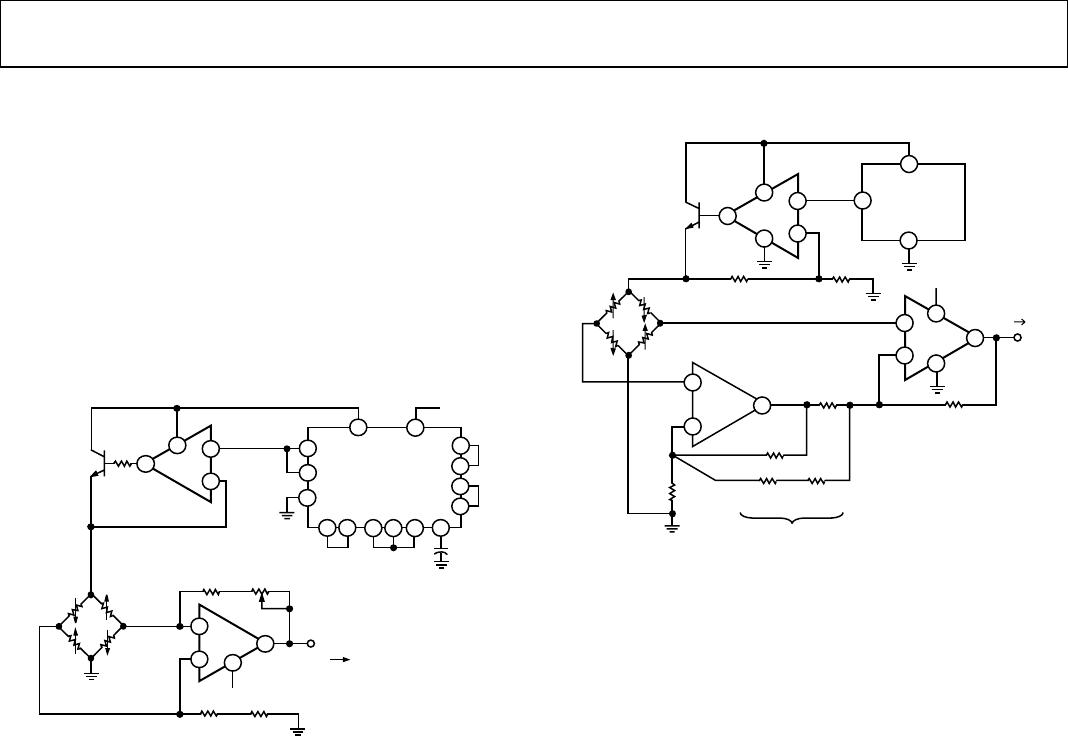
A LOW VOLTAGE, SINGLE SUPPLY STRAIN GAGE
AMPLIFIER
The true zero swing capability of the OPx13 family allows the
amplifier in
Figure 42 to amplify the strain gage bridge
accurately even with no signal input while being powered by a
single 5 V supply. A stable 4 V bridge voltage is made possible
by the rail-to-rail OP295 amplifier, whose output can swing to
within a millivolt of either rail. This high voltage swing greatly
increases the bridge output signal without a corresponding
increase in bridge input.
3
2
8
1
2N2222A
2.5V
1/2
OP295
4
2
4
6
IN
OUT
GND
REF43
4V
5
V
1/2
OP213
1
3
2
8
6
5
4
7
R4
100k
R3
20k
R6
27.4
R5
2.1k
R2
20k
R1
100k
1/2
OP295
R
G
= 2127.4
5V
OUTPUT
0V 3.5V
+
+
350
35mV
FS
R8
12k
R7
20k
+
00286-041
Figure 42. Single Supply Strain Gage Amplifier
A HIGH ACCURACY LINEARIZED RTD
THERMOMETER AMPLIFIER
Zero suppressing the bridge facilitates simple linearization of
the resistor temperature device (RTD) by feeding back a small
amount of the output signal to the RTD. In
Figure 43, the left
leg of the bridge is servoed to a virtual ground voltage by
Amplifier A1, and the right leg of the bridge is servoed to 0 V
by Amplifier A2. This eliminates any error resulting from
common-mode voltage change in the amplifier. A 3-wire RTD
is used to balance the wire resistance on both legs of the bridge,
thereby reducing temperature mismatch errors. The 5 V bridge
excitation is derived from the extremely stable AD588 reference
device with 1.5 ppm/°C drift performance.
Linearization of the RTD is done by feeding a fraction of the
output voltage back to the RTD in the form of a current. With
just the right amount of positive feedback, the amplifier output
will be linearly proportional to the temperature of the RTD.
OP113/OP213/OP413
Rev. F | Page 15 of 24
6
5
4
7
A2
R5
4.02k
R7
100
8
+15V
–15V
1/2
OP213
R2
8.25k
R1
8.25k
R3
50
A1
3
2
1
6
4
13
11
12
7 9 8 10
16 2
14
15
1
3
+15
V
15
V
AD588BQ
1/2
OP213
+
+
R
G
FULL SCALE ADJUST
+
R
W1
R
W2
R
W3
V
OUT
(10mV/°C)
–1.5V = –150°C
+5V = +500°C
R9
5k
LINEARITY
ADJUST
@1/2 FS
R8
49.9k
10µ
100
RTD
R4
100
00286-042
Figure 43. Ultraprecision RTD Amplifier
To calibrate the circuit, first immerse the RTD in a 0°C ice bath
or substitute an exact 100  resistor in place of the RTD. Adjust
the zero adjust potentiometer for a 0 V output, and then set R9,
linearity adjust potentiometer, to the middle of its adjustment
range. Substitute a 280.9  resistor (equivalent to 500°C) in
place of the RTD, and adjust the full-scale adjust potentiometer
for a full-scale voltage of 5 V.
To calibrate out the nonlinearity, substitute a 194.07  resistor
(equivalent to 250°C) in place of the RTD, and then adjust the
linearity adjust potentiometer for a 2.5 V output. Check and
readjust the full-scale and half-scale as needed.
Once calibrated, the amplifier outputs a 10 mV/°C temperature
coefficient with an accuracy better than ±0.5°C over an RTD
measurement range of −150°C to +500°C. Indeed the amplifier
can be calibrated to a higher temperature range, up to 850°C.
A HIGH ACCURACY THERMOCOUPLE AMPLIFIER
Figure 44 shows a popular K-type thermocouple amplifier with
cold-junction compensation. Operating from a single 12 V
supply, the OPx13 family’s low noise allows temperature
measurement to better than 0.02°C resolution over a 0°C to
1000°C range. The cold-junction error is corrected by using an
inexpensive silicon diode as a temperature measuring device.
It should be placed as close to the two terminating junctions as
physically possible. An aluminum block might serve well as an
isothermal system.
1
3
2
8
4
12V
+
+
REF02EZ
12V
2 6
4
D1
1N4148
5V
+
0.1µF
++
K-TYPE
THERMOCOUPLE
40.7µVC
R4
5.62k
R3
53.6
R6
200
R2
2.74k
+
1/2
OP213
0V TO 10V
(0°C TO 1000°C)
10µF
0.1µF
R9
124k
R5
40.2k
R1
10.7k
R8
453
00286-043
Figure 44. Accurate K-Type Thermocouple Amplifier
R6 should be adjusted for a 0 V output with the thermocouple
measuring tip immersed in a 0°C ice bath. When calibrating, be
sure to adjust R6 initially to cause the output to swing in the
positive direction first. Then back off in the negative direction
until the output just stops changing.
AN ULTRALOW NOISE, SINGLE SUPPLY
INSTRUMENTATION AMPLIFIER
Extremely low noise instrumentation amplifiers can be built
using the OPx13 family. Such an amplifier that operates from a
single supply is shown in
Figure 45. Resistors R1 to R5 should
be of high precision and low drift type to maximize CMRR
performance. Although the two inputs are capable of operating
to 0 V, the gain of −100 configuration limits the amplifier input
common-mode voltage to 0.33 V.
*ALL RESISTORS ±0.1%, ±25ppm/°C.
+
1/2
OP213
1/2
OP213
5V TO 36
V
GAIN = + 6
+
+
V
OUT
*R4
10k
20k
R
G
V
IN
*R1
10k
*R2
10k
*R3
10k
*R
G
(200 + 12.7)
00286-044
Figure 45. Ultralow Noise, Single Supply Instrumentation Amplifier
SUPPLY SPLITTER CIRCUIT
The OPx13 family has excellent frequency response
characteristics that make it an ideal pseudoground reference
generator, as shown in
Figure 46. The OPx13 family serves as a
voltage follower buffer. In addition, it drives a large capacitor
that serves as a charge reservoir to minimize transient load
changes, as well as a low impedance output device at high
frequencies. The circuit easily supplies 25 mA load current with
good settling characteristics.

OP113ES-REEL

Mfr. #:
Manufacturer:
Analog Devices Inc.
Description:
Instrumentation Amplifiers Low Noise Low Drift SGL-Supply
Lifecycle:
New from this manufacturer.
Delivery:
DHL FedEx Ups TNT EMS
Payment:
T/T Paypal Visa MoneyGram Western Union