OP113/OP213/OP413
Rev. F | Page 4 of 24
E Grade F Grade
Parameter Symbol Conditions Min Typ Max Min Typ Max Unit
AUDIO PERFORMANCE
THD + Noise V
IN
= 3 V rms, R
L
= 2 kΩ,
f = 1 kHz 0.0009 0.0009 %
Voltage Noise Density e
n
f = 10 Hz 9 9 nV/√Hz
f = 1 kHz 4.7 4.7 nV/√Hz
Current Noise Density i
n
f = 1 kHz 0.4 0.4 pA/√Hz
Voltage Noise e
n
p-p 0.1 Hz to 10 Hz 120 120 nV p-p
DYNAMIC PERFORMANCE
Slew Rate SR R
L
= 2 kΩ 0.8 1.2 0.8 1.2 V/μs
Gain Bandwidth Product GBP 3.4 3.4 MHz
Channel Separation V
OUT
= 10 V p-p
R
L
= 2 kΩ, f = 1 kHz 105 105 dB
Settling Time t
S
to 0.01%, 0 V to 10 V step 9 9 μs
1
Long-term offset voltage is guaranteed by a 1000 hour life test performed on three independent lots at 125°C, with an LTPD of 1.3.
2
Guaranteed specifications, based on characterization data.
@ V
S
= 5.0 V, T
A
= 25°C, unless otherwise noted.
Table 2.
E Grade F Grade
Parameter Symbol Conditions Min Typ Max Min Typ Max Unit
INPUT CHARACTERISTICS
Offset Voltage V
OS
OP113 125 175 μV
−40°C T
A
≤ +85°C 175 250 μV
OP213 150 300 μV
−40°C T
A
≤ +85°C 225 375 μV
OP413 175 325 μV
−40°C T
A
≤ +85°C 250 400 μV
Input Bias Current I
B
V
CM
= 0 V, V
OUT
= 2 300 650 650 nA
−40°C T
A
≤ +85°C 750 750 nA
Input Offset Current I
OS
V
CM
= 0 V, V
OUT
= 2
−40°C T
A
≤ +85°C 50 50 nA
Input Voltage Range V
CM
0 4 4 V
Common-Mode Rejection CMR 0 V ≤ V
CM
≤ 4 V 93 106 90 dB
0 V V
CM
≤ 4 V,
−40°C T
A
≤ +85°C 90 87 dB
Large-Signal Voltage Gain A
VO
OP113, OP213,
R
L
= 600 Ω, 2 kΩ,
0.01 V V
OUT
≤ 3.9 V 2 2 V/μV
OP413, R
L
= 600, 2 kΩ,
0.01 V V
OUT
≤ 3.9 V 1 1 V/μV
Long-Term Offset Voltage
1
V
OS
200 350 μV
Offset Voltage Drift
2
∆V
OS
/∆T 0.2 1.0 1.5 μV/°C
OP113/OP213/OP413
Rev. F | Page 5 of 24
E Grade F Grade
Parameter Symbol Conditions Min Typ Max Min Typ Max Unit
OUTPUT CHARACTERISTICS
Output Voltage Swing High V
OH
R
L
= 600 kΩ 4.0 4.0 V
R
L
= 100 kΩ,
−40°C T
A
≤ +85°C 4.1 4.1 V
R
L
= 600 Ω,
−40°C T
A
≤ +85°C 3.9 3.9 V
Output Voltage Swing Low V
OL
R
L
= 600 Ω,
−40°C T
A
≤ +85°C 8 8 mV
R
L
= 100 kΩ,
−40°C T
A
≤ +85°C 8 8 mV
Short-Circuit Limit I
SC
±30 ±30 mA
POWER SUPPLY
Supply Current I
SY
V
OUT
= 2.0 V, no load 1.6 2.7 2.7 mA
I
SY
–40°C T
A
≤ +85°C 3.0 3.0 mA
AUDIO PERFORMANCE
THD + Noise V
OUT
= 0 dBu, f = 1 kHz 0.001 0.001 %
Voltage Noise Density e
n
f = 10 Hz 9 9 nV/√Hz
f = 1 kHz 4.7 4.7 nV/√Hz
Current Noise Density i
n
f = 1 kHz 0.45 0.45 pA/√Hz
Voltage Noise e
n
p-p 0.1 Hz to 10 Hz 120 120 nV p-p
DYNAMIC PERFORMANCE
Slew Rate SR R
L
= 2 kΩ 0.6 0.9 0.6 V/μs
Gain Bandwidth Product GBP 3.5 3.5 MHz
Settling Time t
S
to 0.01%, 2 V step 5.8 5.8 μs
1
Long-term offset voltage is guaranteed by a 1000 hour life test performed on three independent lots at 125°C, with an LTPD of 1.3.
2
Guaranteed specifications, based on characterization data.
OP113/OP213/OP413
Rev. F | Page 6 of 24
ABSOLUTE MAXIMUM RATINGS
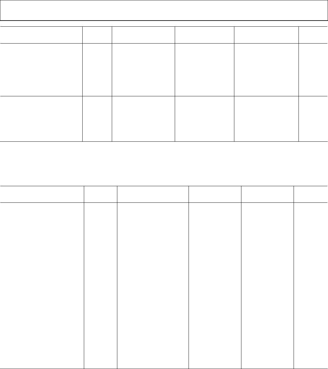
Table 3.
Parameter Rating
Supply Voltage ±18 V
Input Voltage ±18 V
Differential Input Voltage ±10 V
Output Short-Circuit Duration to GND Indefinite
Storage Temperature Range −65°C to +150°C
Operating Temperature Range −40°C to +85°C
Junction Temperature Range −65°C to +150°C
Lead Temperature Range (Soldering, 60 sec) 300°C
Stresses above those listed under Absolute Maximum Ratings
may cause permanent damage to the device. This is a stress
rating only; functional operation of the device at these or any
other conditions above those indicated in the operational
section of this specification is not implied. Exposure to absolute
maximum rating conditions for extended periods may affect
device reliability.
THERMAL RESISTANCE
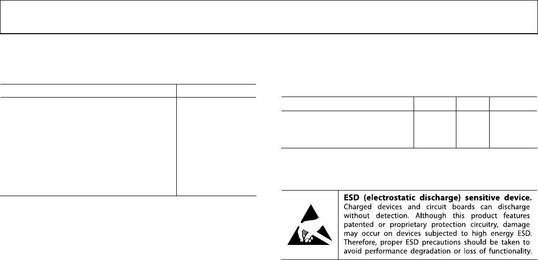
Table 4. Thermal Resistance
Package Type θ
JA
θ
JC
Unit
8-Lead PDIP (P) 103 43 °C/W
8-Lead SOIC_N (S) 158 43 °C/W
16-Lead SOIC_W (S) 92 27 °C/W
ESD CAUTION

OP113ES-REEL

Mfr. #:
Manufacturer:
Analog Devices Inc.
Description:
Instrumentation Amplifiers Low Noise Low Drift SGL-Supply
Lifecycle:
New from this manufacturer.
Delivery:
DHL FedEx Ups TNT EMS
Payment:
T/T Paypal Visa MoneyGram Western Union