ADV7123
Rev. D | Page 10 of 24
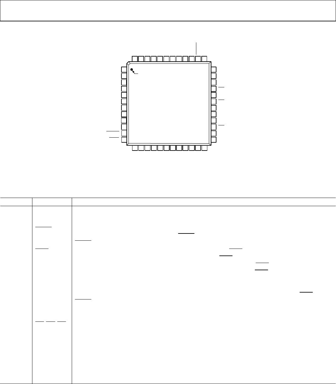
PIN CONFIGURATION AND FUNCTION DESCRIPTIONS
V
AA
B0
B1
B2
B3
B4
B5
B6
B7
B8
B9
CLOCK
R9
R8
R7
R6
R5
R4
R3
R2
R1
R0
PSAVE
R
SET
G0
G1
G2
G3
G4
G5
G6
G7
G8
G9
COMP
V
AA
V
AA
IOB
GND
GND
V
REF
IOB
IOG
IOG
IOR
IOR
BLANK
SYNC
00215-003
48 47 46 45 44 43 42 41 40 39 38 37
35
34
33
30
31
32
36
29
28
27
25
26
2
3
4
7
6
5
1
8
9
10
12
11
13
14 15
16
17
18
19 20
21
22 23 24
PIN 1
INDICATOR
ADV7123
TOP VIEW
(Not to Scale)
Figure 3. Pin Configuration
Table 8. Pin Function Descriptions
Pin No. Mnemonic Description
1 to 10,
14 to 23,
39 to 48
G0 to G9,
B0 to B9,
R0 to R9
Red, Green, and Blue Pixel Data Inputs (TTL Compatible). Pixel data is latched on the rising edge of CLOCK. R0,
G0, and B0 are the least significant data bits. Unused pixel data inputs should be connected to either the
regular printed circuit board (PCB) power or ground plane.
11
BLANK
Composite Blank Control Input (TTL Compatible). A Logic 0 on this control input drives the analog outputs,
IOR, IOB, and IOG, to the blanking level. The BLANK
signal is latched on the rising edge of CLOCK. While
BLANK
is a Logic 0, the R0 to R9, G0 to G9, and B0 to B9 pixel inputs are ignored.
12
SYNC
Composite Sync Control Input (TTL Compatible). A Logic 0 on the SYNC input switches off a 40 IRE current
source. This is internally connected to the IOG analog output. SYNC
does not override any other control or
data input; therefore, it should only be asserted during the blanking interval. SYNC is latched on the rising
edge of CLOCK. If sync information is not required on the green channel, the SYNC
input should be tied to
Logic 0.
13, 29, 30 V
AA
Analog Power Supply (5 V ± 5%). All V
AA
pins on the ADV7123 must be connected.
24 CLOCK
Clock Input (TTL Compatible). The rising edge of CLOCK latches the R0 to R9, G0 to G9, B0 to B9, SYNC
, and
BLANK
pixel and control inputs. It is typically the pixel clock rate of the video system. CLOCK should be driven
by a dedicated TTL buffer.
25, 26 GND Ground. All GND pins must be connected.
27, 31, 33
IOB
, IOG, IOR Differential Red, Green, and Blue Current Outputs (High Impedance Current Sources). These RGB video
outputs are specified to directly drive RS-343A and RS-170 video levels into a doubly terminated 75 Ω load. If
the complementary outputs are not required, these outputs should be tied to ground.
28, 32, 34 IOB, IOG, IOR
Red, Green, and Blue Current Outputs. These high impedance current sources are capable of directly driving a
doubly terminated 75 Ω coaxial cable. All three current outputs should have similar output loads whether or
not they are all being used.
35 COMP
Compensation Pin. This is a compensation pin for the internal reference amplifier. A 0.1 μF ceramic capacitor
must be connected between COMP and V
AA
.
36 V
REF
Voltage Reference Input for DACs or Voltage Reference Output (1.235 V).

