ADV7123
Rev. D | Page 7 of 24
Parameter Min Typ Max Unit
Total Harmonic Distortion
f
CLK
= 50 MHz; f
OUT
= 1.00 MHz
T
A
= 25°C 66 dBc
T
MIN
to T
MAX
65 dBc
f
CLK
= 50 MHz; f
OUT
= 2.00 MHz 64 dBc
f
CLK
= 100 MHz; f
OUT
= 2.00 MHz 64 dBc
f
CLK
= 140 MHz; f
OUT
= 2.00 MHz 55 dBc
DAC PERFORMANCE
Glitch Impulse 10 pV-sec
DAC-to-DAC Crosstalk
3
23 dB
Data Feedthrough
4,
5
22 dB
Clock Feedthrough
4,
5
33 dB
1
These maximum/minimum specifications are guaranteed by characterization over the 3.0 V to 3.6 V range.
2
Note that the ADV7123 exhibits high performance when operating with an internal voltage reference, V
REF
.
3
DAC-to-DAC crosstalk is measured by holding one DAC high while the other two are making low-to-high and high-to-low transitions.
4
Clock and data feedthrough is a function of the amount of overshoot and undershoot on the digital inputs. Glitch impulse includes clock and data feedthrough.
5
TTL input values are 0 V to 3 V, with input rise/fall times of −3 ns, measured at the 10% and 90% points. Timing reference points are 50% for inputs and outputs.
5 V TIMING SPECIFICATIONS
V
AA
= 5 V ± 5%,
1
V
REF
= 1.235 V, R
SET
= 560 Ω, C
L
= 10 pF. All specifications T
MIN
to T
MAX
,
2
unless otherwise noted, T
J MAX
= 110°C.
Table 5.
Parameter
3
Symbol Min Typ Max Unit Conditions
ANALOG OUTPUTS
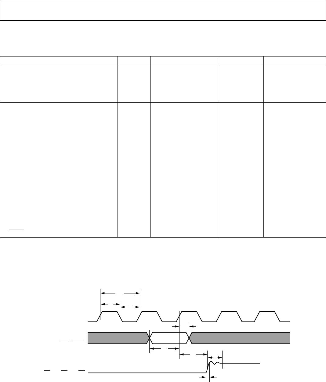
Analog Output Delay t
6
5.5 ns
Analog Output Rise/Fall Time
4
t
7
1.0 ns
Analog Output Transition Time
5
t
8
15 ns
Analog Output Skew
6
t
9
1 2 ns
CLOCK CONTROL
CLOCK Frequency
7
f
CLK
0.5 50 MHz 50 MHz grade
0.5 140 MHz 140 MHz grade
0.5 240 MHz 240 MHz grade
Data and Control Setup t
1
0.5 ns
Data and Control Hold t
2
1.5 ns
CLOCK Period t
3
4.17 ns
CLOCK Pulse Width High t
4
1.875 ns f
CLK_MAX
= 240 MHz
CLOCK Pulse Width Low t
5
1.875 ns f
CLK_MAX
= 240 MHz
CLOCK Pulse Width High t
4
2.85 ns f
CLK_MAX
= 140 MHz
CLOCK Pulse Width Low t
5
2.85 ns f
CLK_MAX
= 140 MHz
CLOCK Pulse Width High t
4
8.0 ns f
CLK_MAX
= 50 MHz
CLOCK Pulse Width Low t
5
8.0 ns f
CLK_MAX
= 50 MHz
Pipeline Delay
6
t
PD
1.0 1.0 1.0 Clock cycles
PSAVE Up Time
6
t
10
2 10
ns
1
These maximum and minimum specifications are guaranteed over this range.
2
Temperature range: T
MIN
to T
MAX
: −40°C to +85°C at 50 MHz and 140 MHz, 0°C to 70°C at 240 MHz.
3
Timing specifications are measured with input levels of 3.0 V (V
IH
) and 0 V (V
IL
) 0 for both 5 V and 3.3 V supplies.
4
Rise time was measured from the 10% to 90% point of zero to full-scale transition, fall time from the 90% to 10% point of a full-scale transition.
5
Measured from 50% point of full-scale transition to 2% of final value.
6
Guaranteed by characterization.
7
f
CLK
maximum specification production tested at 125 MHz; 5 V limits specified here are guaranteed by characterization.