ADV7123
Rev. D | Page 4 of 24
3.3 V SPECIFICATIONS
V
AA
= 3.0 V to 3.6 V, V
REF
= 1.235 V, R
SET
= 560 Ω, C
L
= 10 pF. All specifications T
MIN
to T
MAX
,
1
unless otherwise noted, T
J MAX
= 110°C.
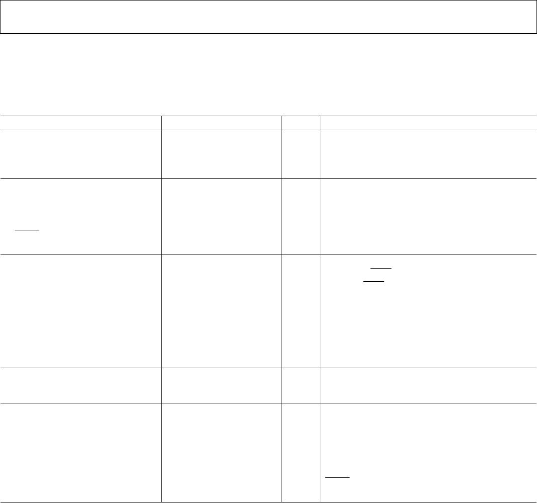
Table 2.
Parameter
2
Min Typ Max Unit Test Conditions
1
STATIC PERFORMANCE
Resolution (Each DAC) 10 Bits R
SET
= 680 Ω
Integral Nonlinearity (BSL) −1 +0.5 +1 LSB R
SET
= 680 Ω
Differential Nonlinearity −1 +0.25 +1 LSB R
SET
= 680 Ω
DIGITAL AND CONTROL INPUTS
Input High Voltage, V
IH
2.0 V
Input Low Voltage, V
IL
0.8 V
Input Current, I
IN
−1 +1 μA V
IN
= 0.0 V or V
DD
PSAVE Pull-Up Current
20 μA
Input Capacitance, C
IN
10 pF
ANALOG OUTPUTS
Output Current 2.0 26.5 mA
Green DAC, SYNC
= high
2.0 18.5 mA
RGB DAC, SYNC
= low
DAC-to-DAC Matching 1.0 %
Output Compliance Range, V
OC
0 1.4 V
Output Impedance, R
OUT
70 kΩ
Output Capacitance, C
OUT
10 pF
Offset Error 0 0 % FSR Tested with DAC output = 0 V
Gain Error
3
0 % FSR FSR = 17.62 mA
VOLTAGE REFERENCE, EXTERNAL
Reference Range, V
REF
1.12 1.235 1.35 V
VOLTAGE REFERENCE, INTERNAL
Voltage Reference, V
REF
1.235 V
POWER DISSIPATION
Digital Supply Current
4
2.2 5.0 mA f
CLK
= 50 MHz
6.5 12.0 mA f
CLK
= 140 MHz
11 15 mA f
CLK
= 240 MHz
16 mA f
CLK
= 330 MHz
Analog Supply Current 67 72 mA R
SET
= 560 Ω
8 mA R
SET
= 4933 Ω
Standby Supply Current 2.1 5.0 mA
PSAVE
= low, digital, and control inputs at V
DD
Power Supply Rejection Ratio 0.1 0.5 %/%
1
Temperature range T
MIN
to T
MAX
: −40°C to +85°C at 50 MHz and 140 MHz, 0°C to 70°C at 240 MHz and 330 MHz.
2
These maximum/minimum specifications are guaranteed by characterization to be over the 3.0 V to 3.6 V range.
3
Gain error = {(Measured (FSC)/Ideal (FSC) − 1) × 100}, where Ideal = V
REF
/R
SET
× K × (0x3FFH) and K = 7.9896.
4
Digital supply is measured with a continuous clock that has data input corresponding to a ramp pattern and with an input level at 0 V and V
DD
.