Data Sheet ADM1073
Rev. B | Page 15 of 24
SENSE
The SENSE pin is used for sensing the voltage across an
external power sense resistor. This voltage is differentially
measured with respect to V
EE
, and used to control the GATE.
If SENSE is lower than 100 mV (after the soft start time), the
GATE pin is allowed to increase up to 12 V to provide
maximum FET enhancement. If the current increases such that
the SENSE pin tries to go above 100 mV, the GATE pin is
controlled in a feedback loop to ensure that the voltage across
the sense resistor is regulated at exactly 100 mV.
SENSE RESISTOR
The ADM1073’s current limiting function can operate at
different current levels. The current limit is determined by
selection of the sense resistor, R
SENSE
. Table 4 shows how the
maximum allowable load current (I
LOAD(MAX)
) and the minimum
and maximum inrush currents (I
LIMIT(MIN)
and I
LIMIT(MAX)
) are
related to the value of R
SENSE
.
Table 4. Minumum and Maximum Inrush Current and Load
Current Levels for Different Values of R
SENSE
R
SENSE
(mΩ) I
LOAD(MAX)
(A) I
LIMIT(MIN)
(A) I
LIMIT(MAX)
(A)
5 17.20 19.40 20.60
10 8.60 9.70 10.30
15 5.73 6.47 6.87
18 4.78 5.39 5.72
22 3.91 4.41 4.68
33 2.61 2.94 3.12
47 1.83 2.06 2.19
51
1.69
1.90
2.02
68 1.26 1.43 1.51
75 1.15 1.29 1.37
90 0.96 1.08 1.14
SOFT START (SS PIN)
The SS pin is used to determine the inrush current profile.
A capacitor should be attached to this pin. Whenever the FET
is requested to turn on, the SS pin is held at ground until the
SENSE pin reaches a few mV. A current source is then turned
on, which linearly ramps the capacitor up to 2.5 V. The
reference voltage for the GATE linear control amplifier is
derived from the soft start voltage, such that the inrush linear
current limit is defined as
SENSE
STARTSOFTLIMIT
RVI ×= 20/
_
Overdriving the SS Pin
The SS pin can be overdriven externally from 0.360 V to 1.95 V
to offset the current limit control loop threshold from 18 mV to
100 mV. This allows different current limits to be selected at
different points of operation without using multiple sense
resistors. The current limit voltage is clamped at 100 mV
maximum.
GATE
Analog output for driving the external FET gate. This pin is
switched to V
EE
when the FET is off, is linearly controlled when
the FET is at the programmed inrush current limit, and is
switched to V
IN
when the FET is fully enhanced. The source
current capability is small to provide slow controlled turn-on,
and the sink current capability is large to provide fast turn-off.
V
IN
Positive supply pin. This current-driven supply is shunt-
regulated at 12.3 V internally, and should be connected to the
most positive input supply terminal (usually −48 V RTN or 0 V)
through a dropper resistor. The resistor should be chosen such
that it always supplies enough current to overcome the
maximum quiescent supply current of the chip. Default R
DROP
=
30 kΩ.
V
EE
Negative supply input. This pin should be connected directly to
the most negative input supply terminal (−48 V). This pin is
also used for differentially sensing across the external power
resistor, and should, therefore, be connected as close to the
sense resistor as possible. (See the Kelvin Sense Resistor
Connection section.)
TIMING CONTROLTIMER
The TIMER pin is an analog pin that determines the maximum
on-time when the FET is in linear current limit, and controls
the PWM duty cycle for pulsed load capacitor charging. A
capacitor should be attached to this pin. When the FET is in
current limit, a 19 µA current source charges the external
capacitor. If the FET is still in current limit when the TIMER
capacitor reaches 2.5 V, the GATE driver is turned off and a
1 µA discharge current sink is turned on. The GATE remains
low until the TIMER capacitor is reduced to 0.5 V. At this point,
the GATE pin is turned on again. If the FET goes back into
current limit, the TIMER recharging starts again.
The PWM duty cycle is set at 6% default level by the size of
these two current sources. Adding a resistor from TIMER to V
EE
decreases the duty cycle. Adding a resistor from TIMER to V
IN
increases the duty cycle.
In addition, a current proportional to the current into the
DRAIN pin is added to the charging current. The additional
current varies linearly with DRAIN voltage. This reduces the
maximum on-time and the percentage PWM duty cycle when
there is a large voltage across the FET.
ADM1073 Data Sheet
Rev. B | Page 16 of 24
DRAIN
Analog input fed by a resistor connected to the drain of the
FET. This pin is clamped to go no higher than 4 V with respect
to V
EE.
Below this level, the voltage on the pin is monitored so
that, if it falls below 2 V, the
PWRGD
output can be set. Above
the 4 V level, the current into the pin is detected and used to
modulate the maximum on-time for the linear FET driver. This
is done by summing a proportion of the drain input current
with the charging current for the TIMER timing capacitor,
thereby reducing the allowable on-time.
PWRGD
Output to indicate when the load capacitor is fully charged.
This is an open collector output with internal pull-up to V
IN
.
When a normal startup is initiated, the
PWRGD
output is
latched low when the DRAIN pin falls below 2 V. The latch is
reset, if either the input supply goes out of range or a current
limit time-out event occurs. The second of these cases ensures
that, if a voltage step of greater than 2 V is presented at the
input, the
PWRGD
flag does not go high while the load
capacitor is being charged up to the additional voltage.
LATCHED
Output to indicate when the device has completed the maxi-
mum number (7) of PWM cycles. This is an open collector
output with an internal current source pull-up. If this PWM
time-out event occurs, the GATE pin is latched low and the
LATCHED
output is set low. This condition can then be reset
by either a power cycling event or a low signal to either the
SHDN
input or the
RESTART
input. By connecting the
LATCHED
signal directly to
SHDN
, the device can effectively
be put into a continuous PWM mode. By connecting the
LATCHED
signal directly to
RESTART
, the device can
effectively be put into autoretry mode, with a 5-second cooling
period.
SPLYGD
Output to indicate when the input supply is within the pro-
grammed voltage window. This is an open collector output with
an internal pull-up current source. For very large capacitive
loads where multiple FETs and controllers are required to meet
the inrush requirements, this output can be used to drive
directly into the UV pin of a second controller. This allows the
second FET to start 1 ms after the first one, with the added
advantage that the input supply UV detection is done on one
controller only. The
SPLYGD
output is asserted only when the
ADM1073 is not in reset mode.
RESTART
Edge-triggered input. Allows the user to remotely command a
5-second shutdown and restart of the hot swap function,
effectively simulating a board removal and replacement. The
shutdown function is triggered by a low pulse of at least 5 µs at
the pin. This pin has an internal pull-up of approximately 6 µA,
allowing it to be driven by an open collector pull-down output
or a push-pull output. The input threshold is 1.5 V.
SHDN
Level-triggered input. Allows the user to command a shutdown
of the hot swap function. When this input is set low, the GATE
output is switched to V
EE
to turn the FET off. This pin has an
internal pull-up of approximately 6 µA, allowing it to be driven
by an open collector pull-down output or a push-pull output.
The input threshold is 1.5 V.
UNDERVOLTAGE/OVERVOLTAGE DETECTION
The ADM1073 incorporates dual pin undervoltage and
overvoltage detection, with a programmable operating voltage
window. When the voltage on the UV pin falls below the UV
falling threshold or the voltage on the OV pin rises above the
OV rising threshold, a fault signal is generated that disables the
linear current regulator and results in the GATE pin being
pulled low. The voltage fault signal is time filtered so that faults
of a duration less than the UV glitch filter time (0.6 ms) and OV
glitch filter time (5 µs) do not force the gate drive low. The filter
operates only on the faulting edge, that is, on a high-to-low
transition on the undervoltage monitor and on a low-to-high
transition on the overvoltage monitor.
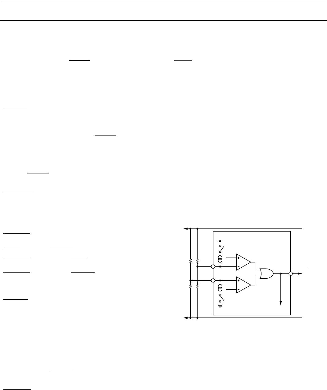
04488-033
1.93V
868mV
UNDERVOLT
AGE
DETECTOR
OVE
RVOLT
AGE
DETECTOR
ADM1073
FET DRIVE
ENABLE
SPLYGD
48V RTN
48V IN
R4
R3
R
2
R1
OV
UV
V
IN
Figure 33. Undervoltage and Overvoltage Circuitry
(Standard 4-Resistor Configuration)
The operating voltage window is determined by selecting the
resistor ratios R1/R2 and R3/R4. These resistor networks form
two resistor dividers that generate the voltages at the UV and
OV pins, which are proportional to the supply voltage. By
choosing these ratios carefully, the user can program the
ADM1073 to apply the supply voltage to the load only when it is
within specific thresholds. Note that 1% tolerance resistors
should always be used to maintain the accuracy of the pro-
grammed thresholds.
Data Sheet ADM1073
Rev. B | Page 17 of 24
UV (Undervoltage)
The voltage on the UV pin is compared to an internal 0.868 V
reference. For the implementation in Figure 33, the undervolt-
age level is then set as
V
UV
= 0.868 × (R1 + R2)/R2
If the UV pin voltage is less than 0.868 V and the comparator
trips, an internal 5 µA current sink is turned on. This pulls the
UV voltage down by
V
UVHYST(PIN)
= 5 µA × R1 × R2/(R1 + R2)
at the UV pin, or by
V
UVHYST(SUPPLY)
= 5 µA × R1
at the supply.
In this manner, the user can program the value of the voltage
hysteresis by varying the parallel impedance of the resistor
divider. The UV comparator has an internal 0.6 ms time delay
to prevent nuisance shutdowns under noisy supply conditions.
OV (Overvoltage)
The voltage on the UV pin is compared to an internal 1.93 V
reference. For the implementation in Figure 33, the overvoltage
level is then set as
V
OV
= 1.93 × (R3 + R4)/R4
If the OV pin voltage exceeds 1.93 V and the comparator trips,
an internal 5 µA current source is turned on. This pulls the OV
voltage up by
V
OVHYST(PIN)
= 5 µA × R3 × R4/(R3 + R4)
at the OV pin, or by
V
OVHYST(SUPPLY)
= 5 µA × R3
at the supply.
In this manner, the user can program the value of the voltage
hysteresis by varying the parallel impedance of the resistor
divider. The OV comparator has an internal 5 µs time delay.
If the voltage on UV or OV goes out of range (below 0.868 V on
UV or above 1.93V on OV), GATE is pulled low. If the supply
subsequently reenters the operating voltage window, the
ADM1073 restores the GATE drive.
Hysteresis must be considered when reentering the operating
window, that is, V
UV
must increase above
0.868 V + V
UVHYST(SUPPLY)
when recovering from an undervoltage fault, and V
OV
must
drop below
1.93 V − V
OVHYST(SUPPLY)
when recovering from an overvoltage fault for GATE to be
restored.
Alternative UV and OV Configurations
A 2-resistor or a 3-resistor implementation can also be used to
set the UV and OV levels (see Figure 34 and Figure 35).
04488-034
ADM1073
48V RTN
48V IN
R2
R1
OV
UV
Figure 34. 2-Resistor UV/OV Implementation
04488-035
ADM1073
48V RTN
48V IN
R3
R1
R2
OV
UV
Figure 35. 3-Resistor UV/OV Implementation

ADM1073ARU-REEL

Mfr. #:
Manufacturer:
Analog Devices Inc.
Description:
Hot Swap Voltage Controllers Full Featured -48V Hot Swap Ctrl'r I.C.
Lifecycle:
New from this manufacturer.
Delivery:
DHL FedEx Ups TNT EMS
Payment:
T/T Paypal Visa MoneyGram Western Union