ADM1073 Data Sheet
Rev. B | Page 6 of 24
ABSOLUTE MAXIMUM RATINGS
All voltages referred to V
EE
, T
A
= 25°C, unless otherwise noted.
Table 2.
Parameter Rating
Supply Voltage (V
DD
− V
EE
) −0.3 V to −200.0 V
Maximum Shunt Supply Voltage, V
SS
16 V
SENSE Pin −2 V to +2 V
GATE Pin −0.3 V to +16 V
UV Pin −0.3 V to +6 V
OV Pin −0.3 V to +6 V
SS Pin
−0.3 V to +6 V
TIMER Pin −0.3 V to +6 V
DRAIN Pin −0.3 V to +6 V
SHDN
Pin −0.3 V to +16 V
SPLYGD
Pin −0.3 V to +16 V
LATCHED
Pin −0.3 V to +16 V
PWRGD
Pin −0.3 V to +16 V
RESTART
Pin −0.3 V to +16 V
Maximum Junction Temperature 125°C
Operating Temperature Range −40°C to +85°C
Continuous Power Dissipation 180 mW
Storage Temperature Range
−65°C to +150°C
Lead Temperature (Soldering, 10 s) 300°C
Stresses above those listed under Absolute Maximum Ratings
may cause permanent damage to the device. This is a stress
rating only and functional operation of the device at these or
any other conditions above those indicated in the operational
section of this specification is not implied. Exposure to absolute
maximum rating conditions for extended periods may affect
device reliability.
THERMAL CHARACTERISTICS
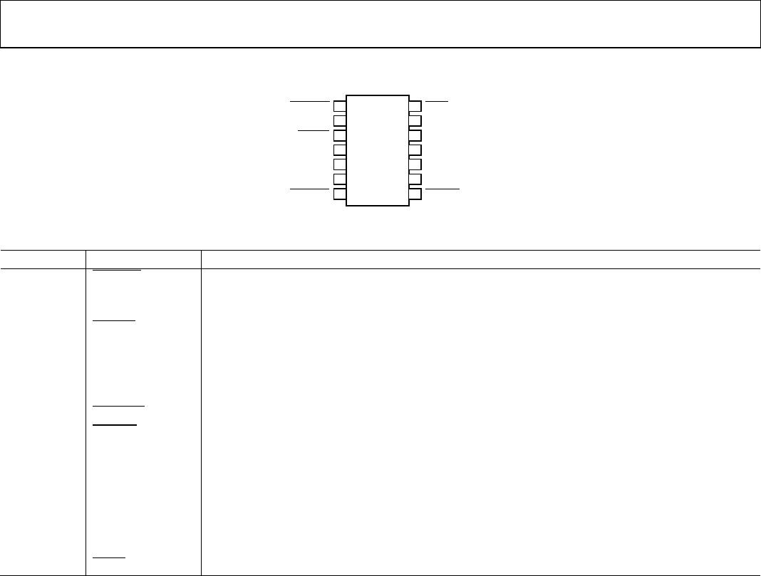
14-lead TSSOP Package:
θ
JA
= 240°C/W
θ
JC
= 43°C/W
ESD CAUTION
ESD (electrostatic discharge) sensitive device. Electrostatic charges as high as 4000 V readily accumulate on
the human body and test equipment and can discharge without detection. Although this product features
proprietary ESD protection circuitry, permanent damage may occur on devices subjected to high energy
electrostatic discharges. Therefore, proper ESD precautions are recommended to avoid performance
degradation or loss of functionality.
Data Sheet ADM1073
Rev. B | Page 7 of 24
PIN CONFIGURATION AND FUNCTION DESCRIPTIONS
ADM1073
TOP VIEW
(Not to Scale)
RESTART
1
V
IN
2
PWRGD
3
SS
4
SENSE
5
SHDN
TIMER
UV
OV
DRAIN
14
13
12
11
10
V
EE
6
LATCHED
7
GATE
SPLYGD
9
8
04488-002
Figure 2. Pin Configuration
Table 3. Pin Function Descriptions
Pin Number
Mnemonic
Function
1
RESTART
Input Pin. Edge-triggered 5-second shutdown and automatic restart.
2 V
IN
Shunt Regulated Positive Supply to Chip. Connect to the positive supply rail via shunt resistor. A 1 µF
capacitor to V
EE
is recommended on the V
IN
pin.
3
PWRGD
Open Drain Output. Signals that the hot swap is complete.
4 SS Analog Pin for Soft Start. An external capacitor on this pin sets the ramp rate of the inrush current
profile. This pin can be overdriven to alter the current limit control loop threshold.
5 SENSE Voltage Input from External Sense Resistor.
6
V
EE
Ground Supply to Chip (usually a 48 V system supply). Also low-side sense resistor connection.
7
LATCHED
Open Drain Output. Signals the end of the PWM retry period after a current fault.
8
SPLYGD
Open Drain Output. Signals that the device is not in reset and that the supply is in operating voltage
window.
9 GATE Output to External FET Gate Drive.
10
DRAIN
Analog Input for Monitoring of FET Drain Voltage.
11 OV Input Pin for Overvoltage Detection Circuitry.
12 UV Input Pin for Undervoltage Detection Circuitry.
13 TIMER Analog Pin. An external capacitor on this pin sets the maximum allowable time in current limit, the
PWM on-time, and the PWM duty cycle.
14
SHDN
Input Pin. Level-triggered device shutdown and reset.
ADM1073 Data Sheet
Rev. B | Page 8 of 24
TYPICAL PERFORMANCE CHARACTERISTICS
04488-003
TEMPERATURE (°C)
8550352051025405570
I
IN
(
A)
0
500
450
400
350
300
250
200
150
100
50
Figure 3. I
IN
vs. Temperature
04488-004
V
IN
(V)
0.5
1.5
2.5
3.5
4.5
5.5
6.5
7.5
8.5
9.5
10.5
11.5
12.5
13.5
14.5
I
IN
(mA)
0.1
100.0
10.0
1.0
T
A
= +85°C
T
A
= +25°C
T
A
= –40°C
Figure 4. I
IN
vs. V
IN
04488-005
TEMPERATURE (°C)
85–50 –35 –20 –5 10 25 40 55 70
R
Z
(
)
0
10
7
8
9
3
4
5
6
1
2
Figure 5. R
Z
(V
IN
Forward Voltage) vs. Temperature
04488-006
TEMPERATURE (°C)
85–50 –35 –20 –5 10 25 40 55 70
V
IN
(V)
11.0
14.5
14.0
13.5
13.0
12.5
12.0
11.5
Figure 6. V
IN
vs. Temperature
04488-007
TEMPERATURE (°C)
85–50 –35 –20 –5 –10 25 40 55 70
V
LKO
(V)
0
12
8
10
4
6
2
Figure 7. Undervoltage Lockout, V
LKO
, vs. Temperature
04488-008
TEMPERATURE (°C)
85–50 –35 20 –50 10 25 40 55 70
DELAY (ms)
0
400
250
300
350
150
200
100
50
Figure 8. POR Delay vs. Temperature

ADM1073ARU-REEL

Mfr. #:
Manufacturer:
Analog Devices Inc.
Description:
Hot Swap Voltage Controllers Full Featured -48V Hot Swap Ctrl'r I.C.
Lifecycle:
New from this manufacturer.
Delivery:
DHL FedEx Ups TNT EMS
Payment:
T/T Paypal Visa MoneyGram Western Union